Introduction
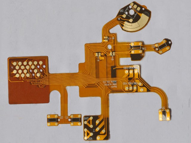
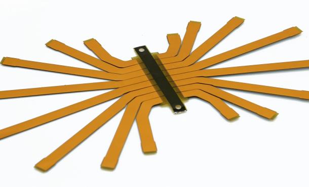
Flex PCBs (flexible printed circuit boards) have become increasingly popular in recent years due to their many advantages over rigid PCBs. Flex circuits can bend and flex to fit into tight spaces, move dynamically, and withstand vibration and shock better than rigid boards. This makes them well-suited for use in wearable devices, medical devices, consumer electronics, automotive applications, aerospace systems, and more.
However, designing and prototyping flex PCBs comes with its own set of challenges. The flexible material introduces new considerations around bending radius, dynamic flexing, layer stackup, and more. Additionally, specialized flex PCB assembly and testing is required. This guide will provide a comprehensive overview of flex PCB prototyping, covering key topics such as design, materials, fabrication, assembly, and testing. Following the recommendations in this guide will help ensure your flex PCB prototype meets requirements and performs as intended in your application.
Flex PCB Design Considerations
Designing a successful flex PCB requires accounting for the unique properties and requirements of the flexible material. Here are some key considerations:
Layer Stackup
Typical flex stackups use flexible dielectric materials like polyimide instead of traditional rigid FR-4 material. Polyimide is available in different thicknesses, with thinner material better able to dynamically flex. Common layer counts are 1-4 layers. Key considerations for layer stackup include:
- Dielectric material type and thickness
- Copper weight (typical 1/2 oz to 1 oz for outer layers)
- Stiffener material, if needed
- Adhesive type between layers
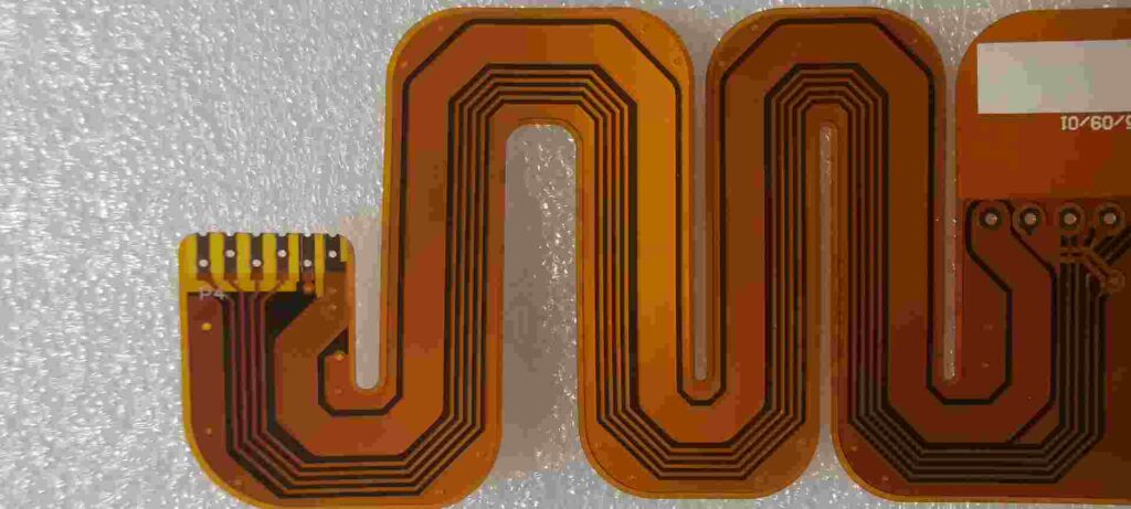
Bending Radius
Flex circuits can bend, but limitations exist based on the stackup. A minimum bend radius helps avoid damage like copper cracking. General guidelines for minimum bend radius:
- 1-2x board thickness for static bends
- 3-10x board thickness for dynamic/repeated bends
Conductor Spacing and Width
Narrow conductor spacing and thin traces add flexibility but can increase resistance. Wider conductors and spacing improves current handling. Aim for:
- 8-10 mil line/space minimum
- 4-6 mil lines for high density
- 8 mil minimum trace width
Stiffeners
Stiffeners made of materials like polyimide can be added to provide localized rigidity. Stiffeners help:
- Maintain planarity
- Prevent localized flexing
- Reduce bending stress
Common locations for stiffeners are connectors, components, and high layer count areas.
Adhesives
Flexible adhesives like acrylic or epoxy are used. Consider adhesive properties during board flexing.
Vias
Use stacked or staggered microvias vs through hole vias which can crack under flexing. Fill vias to avoid air pockets.
Components
Use small, flexible surface mount components rated for flexing. Avoid large, rigid components. Use flexible solder masks under components.
Fabrication and Assembly
Fabricating and assembling flex PCB prototypes requires specialized materials and processes:
Fabrication
- Photolithography machines optimized for flexible substrates
- Etching processes tuned for high-resolution conductors
- Registration capability for tight tolerances
- Layer alignment systems for multilayers
- Specialized test and inspection
Assembly
- Flexible SMT adhesive to allow component flexing
- Small, flexible components
- Reflow process tuned for flex boards
- Conformal coating for durability
- Manual rework may be needed
Using a prototype shop specializing in flex PCBs is recommended. They will have the right capabilities and experience.
Testing Flex PCB Prototypes
Thoroughly testing prototypes is critical to ensure the design and manufacturing processes are reliable. Key tests to consider:
Electrical Testing
- Continuity testing of circuits
- Confirms traces are not cracked or damaged
Continuity Testing Under Bend Conditions
- Bend board to minimum radius while testing continuity
- Verifies conductors remain intact when flexed
Cycle Testing
- Repeatedly flex the board through the expected range of motion
- Assess for degradation in performance
Adhesion Testing
- Apply tape or pulling force to components and traces
- Verify parts and traces remain attached without delamination
Environmental Testing
- Expose prototype to expected humidity, temperature, vibration, etc.
- Confirm boards continue functioning under environmental stress
Failure Analysis
- For prototypes that fail testing, perform root cause analysis
- Look for cracking, delamination, opens, electrical issues
- Inform improvements to design and manufacturing
Thorough prototype testing provides confidence in the flex PCB design, materials, fabrication processes, and robustness for the intended application.
Conclusion
This guide covers key considerations, processes, and testing procedures specific to successfully prototyping flex PCB designs. Flex circuits introduce unique requirements compared to rigid boards. Following the recommendations around design, fabrication, assembly, and testing outlined here will help avoid pitfalls and deliver a functional, high-quality flex PCB prototype that meets the needs of your application. Reach out to a specialist flex PCB manufacturer during your design process to leverage their expertise creating successful prototypes and moving to production.
FQA
What are the main advantages of using flex PCBs vs rigid PCBs?
Some key advantages of flex PCBs include:
- Ability to bend and flex to fit constrained spaces
- Dynamic movement capability
- Improved durability under vibration and shock loads
- Lightweight and thinner than rigid boards
- Eliminates connectors through folded interconnects
- Allows creative industrial design and ergonomics
What are some typical applications suited for flex PCBs?
Flex PCBs are well-suited for:
- Wearable devices
- Medical devices
- Consumer electronics
- Automotive applications
- Aerospace and defense systems
- Industrial Internet of Things (IoT) devices
What are stiffeners and what purpose do they serve?
Stiffeners are rigid sections added to a flex PCB, usually made of material like polyimide. Stiffeners provide localized rigidity to aid in:
- Maintaining overall board planarity
- Preventing unwanted bending in certain areas
- Reinforcing high-layer count regions
- Supporting connectors and components
What is the typical fabrication process for multilayer flex PCBs?
A typical multilayer flex fabrication process includes:
- Laminating adhesive and copper foils to create individual flex core layers
- Photolithography and etching to pattern copper traces on each layer
- Drilling and plating microvias to interconnect layers
- Aligning and laminating the multiple layers together
- Additional photolithography to form outer layer traces
- Final plating, solder mask, and finishing
How is flex PCB assembly different than rigid PCB assembly?
Key differences in flex PCB assembly include:
- Using specialized flexible SMT adhesives
- Smaller, flexible surface mount components
- Reflow process tuned for flex boards
- Conformal coating for durability and flex resistance
- Potential for manual rework due to smaller features


Leave a Reply