What is a Flex PCB?
A flex PCB, also known as a flex circuit or flexible printed circuit board, is a type of printed circuit board that is made of a flexible insulating substrate material. The most common substrate materials used are polyimide or polyester films, such as Kapton or Mylar.
Flex PCBs can be bent, folded, wrapped, or shaped to fit mechanical requirements and three-dimensional spaces. This flexibility allows flex PCBs to be used in many applications where rigid PCBs would be difficult or impossible to integrate.
Benefits of Flex PCBs <h3>
Here are some of the key benefits that make flex PCBs a popular choice in many electronics:
- Flexible – Can conform to different shapes and spaces. Ideal for moving parts and dynamic flexing environments.
- Thin and lightweight – Allows integration into tight spaces and portable devices.
- Durable – Withstands vibration, shock, and repeated bending.
- High reliability – Well-established manufacturing process produces reliable interconnects.
- Efficient routing – Complex routing paths can be produced that are not feasible with rigid PCBs.
- Soft and foldable – Allows customized 3D packaging and cabling.
Flex PCBs open up possibilities that are not possible with standard rigid boards. Their unique set of advantages allow engineers to integrate interconnects in ways that were previously very challenging or not feasible.
Flex PCB Construction and Materials
Although called “flexible”, a flex PCB actually contains both flexible and rigid areas constructed together. Here are the main elements:
- Flexible substrate – Thin insulating base layer that can bend. Made of polyimide or polyester films.
- Conductive traces – Usually copper tracks that are laminated into the substrate. Carry signals between components.
- Cover layer – Protective coating over the conductor layer. Prevents oxidation and damage.
- Stiffeners – Reinforce select areas that require rigidity. Allow connectors and components to be mounted.
- Adhesive – Joins the layers of the flex stackup.
Flex PCB construction showing rigid areas combined with flexible substrate. Image credit: MacroFab
Here are some of the common materials used in flex PCB fabrication:
Substrate Films:
- Polyimide (Kapton) – Most popular. Withstands high temps. Good chemical resistance.
- Polyester (Mylar) – Lower cost. Used for simpler applications.
Conductor Metal:
- Copper – Most common. Excellent conductor and easy to manufacture.
- Aluminum – Lower cost but less conductive than copper.
- Silver – Highest conductivity but much higher cost.
Cover layer films:
- Polyimide
- Liquid Photoimageable Coverlay (LPI)
Stiffeners:
- FR4
- Aluminum
- Polyimide
Bonding Adhesives:
- Acrylic
- Epoxy
- Phenolic Butyral
By selecting the right combination of these materials, flex PCB properties can be tuned for the design requirements of the application.
Flex PCB vs Rigid PCBs
While both flex PCBs and rigid PCBs serve an electrical interconnect function, there are some important differences between the two:
| Parameter | Flex PCB | Rigid PCB |
|---|---|---|
| Composition | Flexible insulating substrate | Rigid insulating substrate (usually FR4) |
| Flexibility | Can conform to 3D shapes | Flat, rigid shape |
| Thickness | Thin from 12 um to 200 um typically | Thick from 0.4 mm to 1.6 mm typically |
| Layers | Typically 1 or 2 layer | Most are 2 to 16 layers |
| Traces | Pitch can be under 50 um | Pitch typically over 100 um |
| Components | Usually only passive SMT components | Supports passive SMT and thru-hole components |
| Thermal issues | Less due to flexibility | More due to rigidity and higher power |
| Cost | Generally higher | Lower in medium to high volumes |
In summary, flex PCB provide unique advantages of flexibility, thinness, and 3D routing capabilities, while rigid PCBs offer advantages in multilayer board complexity, power handling, and economy.
Flex PCB Design Guidelines
Designing a flex PCB requires following specific guidelines to ensure the flex circuit reliability meets the application requirements over the product lifetime. Here are some key flex PCB design considerations:
Flexural Stresses
Avoid sharp corners or sudden changes in trace directions. Use teardrop pads at junctions between traces. Manage stresses near connectors with anchoring vias.
Trace Width and Spacing
Use wider traces than the minimum required to increase lifetime. Common trace widths are between 0.1mm to 0.3mm. Provide adequate spacing between traces for manufacturing tolerances.
Stiffener Placement
Strategically place stiffeners to manage stresses. Allow enough flex area for dynamic bending applications. Anchor stiffeners when using advanced HDI flex layers.
Component Sizing and Placement
Use smaller, lighter components when possible. Place components intelligently to minimize stresses. Allow space for adhesive fillets around component pads.
Stackup Construction
Select substrate, adhesive, and coverlay materials suited for the required flexibility, lifespan, and reliability. Most flex PCBs are 1 or 2 conductive layers.
Bending Radius
Do not bend flex PCBs tighter than their minimum bending radius specification or traces may fracture over time.
Test and Qualification
Test thoroughly with environmental stress screening, cycling, shock/vibe, temperature extremes to validate the design.
By appropriately considering these design guidelines, flex PCBs can be optimized to meet the mechanical and electrical requirements of dynamic flexing applications.
Flex PCB Manufacturing Process
Flex PCB fabrication involves specialized manufacturing techniques to produce the thin, flexible circuit boards. Here is a simplified overview of the flex PCB manufacturing process steps:
- Design – Create flex PCB design file according to flex design guidelines.
- Film Preparation – Cut flex substrate material such as Kapton or polyester to size. Prepare bonding films.
- Photolithography – Laminate photoresist dry film. Expose with circuit pattern. Develop to form etched pattern.
- Etching – Etch away unwanted copper not protected by photoresist to form traces.
- Stripping – Remove remaining photoresist.
- Die Cutting – Cut individual flex PCB outlines from panel.
- Elongation – Stretch flex PCBs to relieve internal stresses. Improves flex lifetime.
- Solder Mask – Screen print or laminate solder mask over traces for insulation and protection.
- Automated Optical Inspection – Inspect circuit patterns for defects using AOI system.
- Electrical Testing – Validate PCB electrical connections meet specifications.
- Assembly – SMT component assembly and soldering if required.
- Quality Inspection – Visual inspection and functional testing of completed boards.
- Packing and Shipping – Carefully package flex PCBs to avoid damage during transportation.
Flex PCB production requires specialized skills in handling ultra-thin flexible materials and managing stresses in fabrication processes. When produced by an experienced manufacturer, high quality and reliable flex circuits can be manufactured.
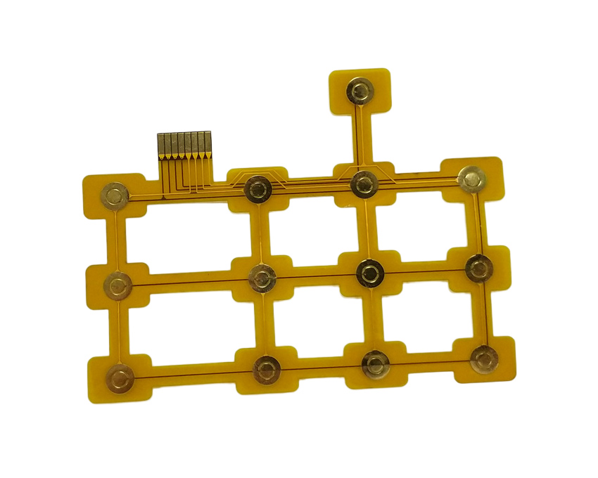
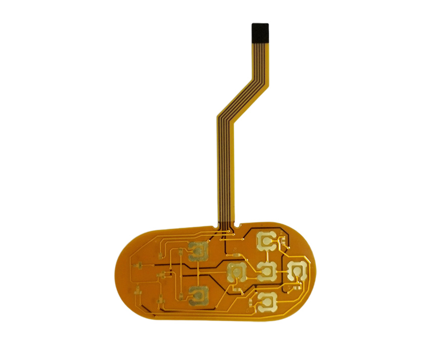
Types of Flex PCBs
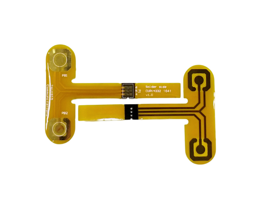
There are several common types and variations of flex PCBs designed for different applications:
Single Layer Flex Circuits
- Simplest construction with a single conductive layer
- Typically use polyimide substrate
- Lowest cost flex PCB option
Double Layer Flex Circuits
- Two conductive layers for more complex routing
- Often used for dynamic cables and interconnects
Multilayer Flex Circuits
- Have 3 or more conductive layers
- Allow high density interconnections
- Used where high complexity is required
Rigid-Flex PCBs
- Combines rigid PCB areas with flexible circuits
- Allows mounting components while still bending
Flexible Cables and Ribbon Cables
- Interconnect cables produced using flex PCB technology
- Pitch can be below 0.5mm
Flexible Heaters
- Flex circuits with resistive heating elements and temperature sensors
- Can heat surfaces that rigid PCBs cannot fit
With creative construction and materials selection, flex PCBs can be architected in many configurations to suit the mechanical, electrical, and reliability needs of the application.
Flex PCB Applications
Some of the common applications where flex PCBs are used include:
- Consumer electronics
- Cell phones, laptops, tablets
- Cameras, wearables
- Displays
- Automotive electronics
- Dashboard display flex cables
- Engine control units
- sensors
- Industrial
- Robotics joints and arms
- Machine cabling
- Medical devices
- Military and aerospace
- Guided missiles
- Avionics systems
- Radar systems
- Medical
- Hearing aids
- Patient monitoring
- Medical imaging
Flex circuits provide interconnect solutions where motion, space constraints, production optimization, or reliability drive the need to go beyond the capabilities of rigid boards.
Pros and Cons of Flex PCBs
Pros
- Extremely flexible and foldable
- Thin, lightweight, and customizable
- Vibration and impact resistant
- Complex and dense routing capabilities
- Easy to prototype and make design changes
- Well established manufacturing process
Cons
- Limited component mounting options
- Higher cost compared to rigid PCBs
- Require specialized design know-how
- Longer lead times compared to rigid PCBs
- Prone to wear and fatigue over time
Flex PCB Design Software
Engineers use specialized PCB design software tools for flex and rigid-flex design needs:
- Altium Designer – Leading professional PCB tool with dedicated rigid-flex features.
- Cadence Allegro PCB Editor – Advanced tool with integrated flex and rigid-flex capabilities.
- Mentor Xpedition – Flex and rigid flex design features for the complete PCB workflow.
- Zuken CR-8000 – Designed for flex and rigid-flex with advanced routing tools.
- Pads Professional – Low cost design solution with basic flex and rigid-flex support.
Flex PCB designers need tools that make it as straightforward as possible to manage the intricacies of flex and rigid-flex constructions. Integrated solutions from leading vendors provide the capabilities to architect complex flex and rigid-flex boards.
Choosing A Flex PCB Manufacturer
What should you look for when selecting a flex PCB supplier?
- Experience – Seek an established company focused on flex and rigid-flex PCBs. They will have the know-how to build robust, reliable designs and manage the nuances of flexible circuits.
- Quality – Ensure the manufacturer has effective quality systems in place and inspects both product and processes. This results in consistent, defect-free flex PCBs.
- Technical Support – Select a supplier that provides design reviews and upfront DFM guidance. Their expertise can improve your design’s manufacturability.
- Certifications – Look for technical certifications such as ISO 9001. These reflect disciplined quality systems and controls.
- Prototyping Capabilities – Choose a supplier that can quickly turn prototype flex designs so iterations are faster.
- Flexible and Responsive – Your flex PCB partner should be easy to work with and responsive throughout the design and manufacturing stages.
Do your due diligence to select a flex PCB company that best fits your needs in terms of capabilities, responsiveness, expertise, and value.
Flex PCB Design Guidelines Infographic
Here is a helpful infographic summarizing key flex PCB design guidelines:
Flex PCB design guidelines – Image credit: All Flex
FAQs
What are some typical applications of flex PCBs?
Some of the most common applications for flex PCBs include consumer electronics, automotive, industrial machinery, aerospace, and medical devices. The need for dynamic flexibility, space-savings, improved reliability, and cabling make flex circuits an attractive option across many industries.
What thickness range do flex PCBs typically come in?
Flex PCB thickness generally ranges from about 12 microns on the low end up to around 200 microns on the high side. Typical flex PCB thickness is around 25 to 75 microns. Rigid sections are usually thicker FR4 areas in the 0.4 to 1.6mm range when constructed as rigid-flex boards.
How many conductive layers can you get on a flex PCB?
The majority of flex PCBs designs have 1 or 2 conductive signal layers. Some high density interconnection flex circuits are designed with 4 to 8 layers. The thinnest flex PCBs tend to be single layer, while multilayer flex provides the highest interconnection density in the smallest space.
What line widths and spaces are achievable with flex PCBs?
The small features possible with flex PCB fabrication allows very fine line width and spacing. Typical trace/space is 100 um (4 mils) and can go down below 50um (2 mils) for high density designs. This compact routing ability makes flex PCBs advantageous compared to standard rigid PCB technology.
Can you mount components on flex PCBs?
Yes, surface mount components can be assembled onto flex PCBs, usually in the designated rigid sections which provide stability for pick and place assembly processes. Avoid placing heavy, bulky through hole components on dynamic areas of the flex circuit which need to bend. SMT components should be anchored well with solder.
What are some ways flex PCBs fail over time?
Common flex PCB failure modes when not designed properly include conductor fractures or cracks from repeated flexing, delamination between material layers, componentPad lift off due to poor adhesion, and stresses around interfaces with rigid sections leading to damaged traces. Proper design and testing is key.
Conclusion
Flex PCBs provide unique advantages of flexibility, 3D routing, reliability, and space savings that are not possible with standard PCB technology. When designed and manufactured correctly using the right materials and process, flex circuits can provide robust interconnection solutions under dynamic conditions over long lifetimes. With the proliferation of consumer electronics, automotive electronics, and advanced industrial and medical systems, the use of flex PCB technology will continue evolving to support design innovation.


Leave a Reply