 flexpcb.org
Bend radius
Check a static screening benchmark. Identify designs that need further engineering review.
Open calculator ↗FLEXIBLE CIRCUITS / PRACTICAL ENGINEERING
Understand the materials. Plan the bend. Build a better quote package. Your starting point for flexible printed circuits, from first layout to fabrication.
THE BASICS, WITHOUT THE GUESSWORK
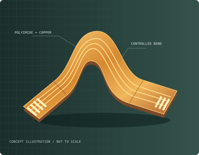
A flex PCB is a printed circuit built on a flexible dielectric film, with patterned copper that carries signals and power. Polyimide is a common substrate; other films suit particular processes and environments.
Flexibility lets a circuit fit a three-dimensional enclosure. Repeated motion is a separate design requirement: a circuit that bends during installation is not automatically suitable for continuous flexing.
Start with the design guide →ANATOMY / EXAMPLE DOUBLE-SIDED FLEX
Simplified adhesiveless-base construction. Not to scale. Openings, plating and local stiffeners are omitted.
ENGINEERING WORKBENCH
Explore a construction before you send files. Every result shows its assumptions and the next question to take to your fabricator.
Check a static screening benchmark. Identify designs that need further engineering review.
Open calculator ↗See copper, dielectric and coverlay layers. Separate flex thickness from local reinforcement.
Build a stackup ↗Build a material shortlist around motion, temperature, budget and signal requirements.
Compare materials ↗Explore an illustrative budget range. Carry your build parameters into the quote brief.
Estimate a budget ↗CHOOSE THE CONSTRUCTION
Layer count changes routing freedom, total thickness and bending behaviour. A local stiffener and a rigid-flex section serve different purposes.
| Construction | What it gives you | What to check | Explore |
|---|---|---|---|
| Single-sided | One copper layer; a simple interconnect | Routing capacity and bend-life requirements | Single-sided flex → |
| Double-sided | Two copper layers with interlayer connections | Via placement, finished thickness and bend zone | Double-sided flex → |
| Multilayer | Additional routing and reference layers | Bonding construction, stiffness and tolerances | Multilayer flex → |
| Rigid-flex | Integrated rigid component areas and flexible links | Transitions, assembly support and cost | Rigid-flex design → |
MATERIALS
Compare the substrate, copper foil, coverlay adhesive and stiffener together. For repeated motion, specify a copper system and test plan suited to the actual duty cycle.
PI, PET, LCP and copper →DESIGN
Keep pads, vias and components outside the moving bend region. Coordinate trace routing, copper distribution and strain relief with the fabricator before locking the outline.
Design rules and stackups →COST
Panel utilisation, layer count, tooling, stiffeners and inspection affect cost. Compare quotations with the same material, finished thickness and test requirements.
Understand the cost drivers →APPLICATION REQUIREMENTS
These are design use cases, not customer case studies. Identify what your product asks the circuit to survive.
Limited space, skin-adjacent heat and repeated handling.
Design considerations →Traceability, environmental exposure and documented verification.
Build requirements →Vibration, thermal cycling and connector retention.
Reliability questions →Fine-pitch interconnects, shielding and installation geometry.
Interconnect planning →FROM FILES TO FINISHED CIRCUIT
Check files, stackup, bend geometry and acceptance criteria.
Pattern copper and create interlayer connections where required.
Apply the specified bonding films, coverlays and stiffeners.
Complete surface finishing and the circuit outline.
Use the agreed electrical and dimensional inspection plan.
Compare the information requested for flexible PCB manufacturing and custom flexible circuit boards when preparing your fabrication brief.
SPECIFICATIONS THAT CAN BE VERIFIED
IPC-2223 addresses flexible and rigid-flex board design. IPC-6013 addresses qualification and performance. Agree the applicable revision, class and test requirements in procurement documentation.
Layer construction · finished thickness · material grade · copper type · bend radius and cycle target · impedance requirements · inspection criteria · quantity and required date.
Manufacturing limits, certifications and delivery commitments will be shown only after supporting information is confirmed.
PRACTICAL ANSWERS
A flex PCB uses a flexible base through its circuit structure. Rigid-flex integrates rigid board regions with flexible interconnect regions. A stiffener supports a local area of a flex circuit; it does not add the electrically interconnected layers of a rigid-flex section.
No. A bend-to-install design may not survive repeated motion. Dynamic flex requires a review of copper type, geometry, finished thickness, bend direction and cycle-life testing.
No. Conventional coverlay is a dielectric film bonded with adhesive, with openings for connection pads. Flexible solder masks use different materials and processing. Specify the actual protective system and opening tolerances.
Start with fabrication data, a board outline, drill data, stackup and material notes. Add quantities, bend requirements and the required date. For assembly, include the BOM, placement data and assembly drawings.
Board area is only one input. Irregular shapes can reduce panel utilisation; additional layers, tooling, stiffeners and test requirements can increase cost. Compare the full build specification.
Yes. Double-sided and multilayer constructions can use plated interconnections. Keep vias outside moving bend regions and confirm the pad, drill and plating requirements with the fabricator.
Flexible circuits need careful handling, defined bend regions and support during assembly. Tight material and registration requirements can raise fabrication cost. They cannot stretch like an elastomer, and a static design does not automatically meet a repeated-motion requirement.
Price depends on the complete construction, panel utilisation, order quantity, tooling and inspection scope. Use the estimator to explore illustrative budgeting assumptions, then request a written quote based on your fabrication files.
YOUR NEXT STEP
Tell us what the circuit needs to do, how it will bend and when you need it. A complete build brief makes a quote easier to evaluate.
Include Gerber and drill data, a fabrication drawing and stackup notes. Put related files in one ZIP. Add a BOM and placement file when assembly is required.
ENGINEERING LIBRARY
Build a clear flex PCB Gerber manifest for copper, coverlay and stiffener data, then check orientation, missing files and revision consistency before release.
Diagnose lost flex PCB pad area by separating film opening size, registration and adhesive intrusion, with a worked measurement example and trial checklist.
Compare polyimide datasheet values by specimen, thickness, direction, frequency and conditioning, using a practical worksheet and clearly bounded examples.
Separate nominal flex PCB layer inputs from finished regional thickness requirements, with worked examples and a practical measurement agreement worksheet.
Define flex PCB bend-radius and neutral-axis assumptions, then compare copper strain using an original worked example with explicit model limits.
Review automotive camera FPC supports, connector mating and vibration evidence using a six-location load-path worksheet and clear test boundaries.