Introduction
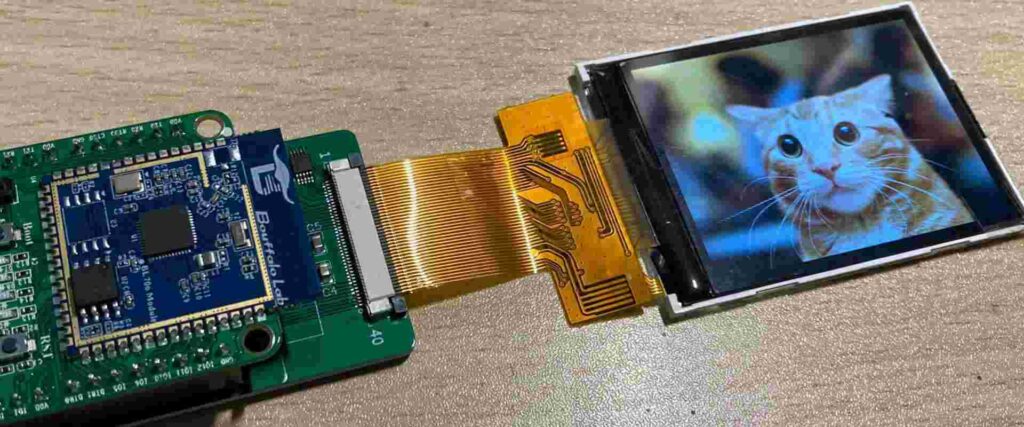
Flex PCBs (flexible printed circuit boards), also known as flex circuits, are printed circuits manufactured on thin, flexible substrates like polyimide or polyester. They provide unique advantages over traditional rigid PCBs, including withstand repetitive bending and can fit in tight spaces. Flex PCBs enable innovative product designs across various industries, especially consumer electronics, automotive, aerospace, and medical devices.
In 2023, flex PCB design requires understanding critical considerations like substrate selection, layer stackup, component placement, trace routing, and more to ensure performance, reliability, and manufacturability. This comprehensive guide will explore best practices for designing successful flex PCBs from concept to production.
Selecting Flexible Substrate Material

Choosing the right flexible substrate is the first critical step in flex PCB design. The substrate defines the fundamental mechanical properties of the circuit, like flexibility, bend radius, chemical resistance, flammability, etc. Common flex substrate options include:
Polyimide
Polyimide films like Kapton from DuPont offer excellent thermal stability and chemical resistance. They have high tensile strength and withstand temperatures up to 400°C. Polyimide allows tight bend radii down to 0.010 in. It is more expensive than other flex substrates but offers the best overall performance.
Polyester
Polyester films like Mylar provide a lower-cost alternative to polyimide. Polyester has relatively good chemical resistance but lower maximum operating temperature around 150°C. It allows bend radii down to 0.020 in. Polyester is suitable for less demanding flex applications.
LCP
Liquid crystal polymer (LCP) films offer very low water absorption compared to polyimide or polyester. LCP allows higher frequency, lower loss electrical performance, albeit at higher cost. It withstands high temperatures up to 280°C. LCP is seen in advanced flex applications like aerospace and defense systems.
PEN
Polyethylene naphthalate (PEN) is a newer high-temperature substrate up to 200°C. It provides better dimensional stability than polyimide. PEN features low moisture absorption and excellent chemical resistance. It is also more eco-friendly and recyclable versus other substrates.
The target application and operating requirements will determine the ideal flexible substrate material for a particular flex PCB design. Polyimide remains the most versatile and widely used.
Layer Stackup
The layer stackup defines the sequence of dielectric and copper foil layers in a flex PCB. A basic stackup includes a flexible dielectric core laminated with copper foil on one or both sides. Standard cores are 25 μm to 100 μm thick. Thicker cores provide better dimensional stability while thinner cores allow tighter bends. Copper foils are typically 12 μm to 35 μm thick.
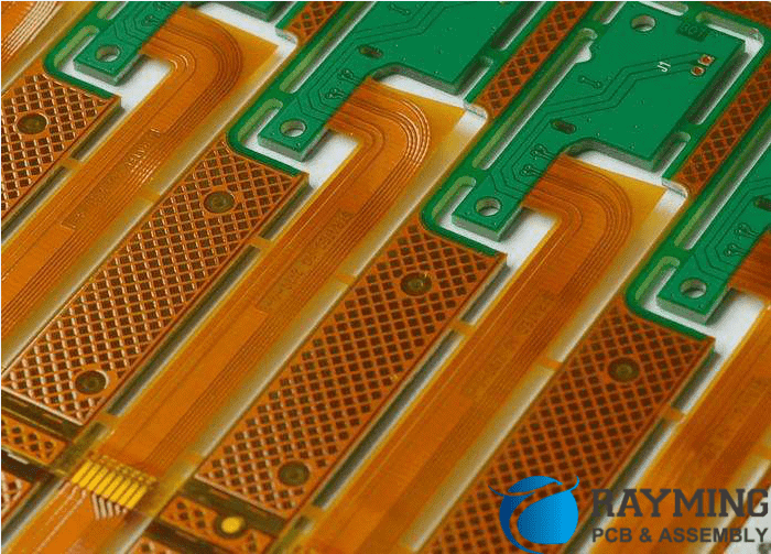
More complex rigid-flex designs may involve multiple flexible cores laminated with rigid FR4 layers to provide local stiffening. Rigid sections allow component mounting while flexible layers interconnect rigid areas and enable dynamic flexing. Careful stackup planning ensures the design can physically bend as intended without damage.
Here is an example 4-layer symmetrical stackup for a polyimide flex PCB:
| Layer | Function | Thickness |
|---|---|---|
| Copper | Outer layer 2 | 18 μm |
| Polyimide | Dielectric core | 50 μm |
| Copper | Inner layer 2 | 18 μm |
| Polyper | Dielectric core | 50 μm |
| Copper | Inner layer 1 | 18 μm |
| Polyimide | Dielectric core | 50 μm |
| Copper | Outer layer 1 | 18 μm |
The stackup provides two signaling layers and references planes for controlled impedance routing. Additional layers can be added for more complex routing needs.
Component Selection and Placement
Component selection and placement are important considerations for flex PCBs:
- Use smaller, lighter surface mount devices (SMD) – Bulky through-hole components can impede flexing and cause failures. SMD packages minimize mass and thickness.
- Avoid large BGAs – Board-to-board connectors are preferred over high-pin count BGAs (> 400 pins) which have potential solder joint reliability issues from flexure.
- Place components strategically – Position inflexible components on rigid sections of rigid-flex. Group components to localize stiffening from solder joints.
- Balance component placement – Distribute components evenly across both sides of the flex PCB to prevent mechanical imbalances when flexing.
- Round sharp component edges – Sharp component edges can wear into flexible substrates during dynamic flexing and cause cracks. Rounded edges help avoid this.
Following placement guidelines optimizes reliability and minimizes stresses on components and joints during flex PCB service life.
Trace Routing
Routing traces on flex PCBs require special considerations versus rigid boards:
- Use teardrop pads – Teardrop solder pads improve trace junction reliability by easing stresses from dynamic flexing.
- Avoid acute trace angles – Acute trace angles concentrate stress. Use rounded corners or 45/90 degree angles instead.
- Keep traces short – Long traces can crack more easily from repetitive bending. Keep traces short, especially near fold lines.
- Plan for controlled impedance – Match trace widths and spacing to dielectric thickness to achieve controlled impedance for high-speed signals.
- Minimize rigid portions – Limit use of stiffeners, solder mask, and thicker copper to only where absolutely needed.
- Verify fold lines – Ensure traces don’t inadvertently cross board fold lines which can lead to cracks.
Following these guidelines when routing flex PCB traces enhances reliability and signal performance.
Protective Coatings
Protective coverlay and solder mask coatings safeguard a flex PCB’s traces and provide electrical insulation:
- Liquid photoimageable solder mask (LPISM) offers excellent flex durability. It is applied like “wet” solder mask on rigid PCBs.
- Coverlay films adhere better to flex PCB substrates compared to LPISM. Popular covers include polyimide, polyester, and silicone. Coverlay effectively seals traces but is less mechanically robust than LPISM.
- Conformal coatings like acrylics or urethanes provide supplemental environmental protection. They shield against moisture, dust, chemicals, etc.
- Selectively apply coatings only in needed areas to maximize flexibility.
Protective coatings are vital for reliability but their use should be balanced with preserving flexing ability.
Flex and Rigid-Flex Assembly

Assembling flex PCBs and rigid-flex boards requires special procedures:
- Dedicated fixtures – Unique fixtures secure thin, flexible boards to prevent warping during assembly. Fixtures also aid post-solder inspection.
- Adhesives – Epoxies and acrylics help bond flex layers during lamination while also providing insulation around drilled holes.
- Special solders – Low temperature solders reduce thermal stress. SAC alloy solders improve flex joint reliability.
- Process control – Tight process controls on parameters like soldering temperature and component placement are needed.
- No wave soldering – Wave solder risks damaging thin flex PCBs. Solder fountain or selective hand soldering should be used instead.
With careful assembly process engineering, flex PCBs and complex rigid-flex can be manufactured successfully.
Testing Flexible Circuits
Verification testing of flex PCBs helps ensure reliability:
- Continuity testing checks for short circuits or opens, especially at joints. Flying probe testers are commonly used.
- Flexure testing checks performance during and after bending repetitively to extremes. Problems like delamination or cracking are detected.
- Environmental testing evaluates resistance to expected operating environments — temperature, humidity, vibration, etc.
- Function testing validates actual circuit performance for analog, digital, and high-speed signals during and after flexing.
- Inspection thoroughly checks solder joints, trace integrity, and overall assembly quality. X-ray inspection excels at detecting hidden flaws.
Start testing early in the design flow to uncover problems and improve the flex PCB layout.
Fabricating Prototypes and Production Flex Circuits
Fabricating initial prototypes is important for verification testing:
- Fast-turn prototypes validate design and fabrication process assumptions. Flex suppliers like FlexPCB and Epec offer 24-48 hour fabrication.
- Low volume supports early prototyping through pilot production. Traditional PCB suppliers or specialty flex shops (AllFlex, Minco) can provide.
Moving to volume production involves:
- Qualifying fabricators – Selecting flex PCB production partners with proven quality and expertise.
- Preparing data packages – Supplying comprehensive Gerber, NC drill, netlist, and assembly files per the fabricator’s requirements.
- Quality oversight – Managing fabrication quality via audit plans, incoming inspections, corrective actions, etc.
With an iterative prototyping-to-production flow, flex PCBs and complete flex assemblies can be manufactured successfully.
Key Flex PCB Design Guidelines Summary
- Choose the optimal flexible substrate material for the application
- Plan appropriate layer stackups for needed conductors and shielding
- Utilize smaller SMD components strategically placed for reliability
- Route traces to avoid acute angles and maximize flex endurance
- Apply protective coatings like LPISM and coverlay selectively
- Develop specialized assembly processes and fixtures
- Verify performance through comprehensive testing
- Partner with experienced flex PCB fabricators for quality results
Following these best practices from design through manufacturing ensures robust, reliable flex circuits.
Flexible PCB Design FAQ
Here are answers to some frequently asked questions about designing flex PCBs:
Q: What are the minimum bend radius and trace spacing rules for common flex substrates?
A: Here are typical minimum bend radii and trace/space rules:
- Polyimide – 0.010 in bend radius; 3/3 mil trace/space
- Polyester – 0.020 in bend radius; 5/5 mil trace/space
- LCP – 0.010 in bend radius; 3/3 mil trace/space
Q: How many layers can be designed with flex PCBs?
A: Flex PCBs typically range from 1 to about 12 layers for the thinnest substrates. Specific layer counts depend on dielectric materials used. Polyimide supports the most layers. Rigid-flex boards can potentially incorporate 20+ layers with embedded rigid sections.
Q: What are recommended minimum voltages for spacing in flex PCB layouts?
A: For polyimide dielectric (~3.4 mil thickness), 5-7 V signals should have >= 5 mil spacing. 15-25 V signals should use >= 10 mil spacing. High voltage spacing rules depend partly on dielectric thickness.
Q: How are components attached to flex PCBs?
A: Surface mount components are attached with solder paste and reflow soldering. Selective hand soldering can also be used. Small through-hole components are sometimes anchored with adhesives. Larger through-hole components should be avoided.
Q: Can flex PCBs be tested like rigid boards?
A: Yes, flex PCBs can undergo similar testing as rigid boards for continuity, shorts/opens using fixtures to secure the thin flex substrates. Automated flying probe testers are commonly used. Functional circuit testing requires flexing while powered.
Q: What are the typical lead times for producing flex PCB prototypes?
A: Quick-turn flex PCB shops can deliver prototype orders in as fast as 24-48 hours. Lead times for prototypes from full service suppliers is typically 5-7 days for simple 2-4 layer flex circuits. More complex rigid-flex may require 2-3 weeks lead time.
Q: When should electrical stiffeners be used in flex PCB layouts?
A: Stiffeners help manage flex PCB stability and prevent unwanted twisting. They are recommended for areas with dense components or routing. Stiffeners can also be used to strengthen high strain areas. But stiffeners should be minimized to preserve flexibility.
Q: What design for manufacturing (DFM) checks should be run on flex PCB layouts?
A: Important DFM checks include: acute angle trace verification; tee junction confirmation; clearance checks between pads, traces, and board outline; hole size/tolerance checks; and annular ring inspections. Running regular DFM analysis avoids assembly issues.


Leave a Reply