Introduction to PCB Manufacturing
Printed Circuit Boards (PCBs) are the backbone of modern electronics. They are used in almost every electronic device, from smartphones and computers to medical equipment and aerospace systems. PCBs provide a platform for electrical components to be connected and interact with each other, enabling the device to function as intended. The PCB manufacturing process is a complex and precise one, requiring specialized equipment and skilled technicians.
In this article, we will explore the Aluminum PCB manufacturing process in a PCB factory, focusing on the key steps involved and the advantages of using aluminum as a substrate material.
What is an Aluminum PCB?
An aluminum PCB is a type of printed circuit board that uses aluminum as the base material instead of the more commonly used FR-4 (a glass-reinforced epoxy laminate). Aluminum PCBs offer several advantages over traditional PCBs, including:
- Excellent Thermal Conductivity: Aluminum dissipates heat more efficiently than FR-4, making it ideal for high-power applications.
- Lightweight: Aluminum is lighter than FR-4, making it suitable for weight-sensitive applications such as aerospace and automotive systems.
- Durability: Aluminum is more resistant to vibration and shock than FR-4, increasing the PCB’s lifespan in harsh environments.
- Electromagnetic shielding: Aluminum provides natural electromagnetic shielding, reducing interference and improving signal integrity.
Aluminum PCB Applications
Aluminum PCBs are used in various industries and applications, including:
- Power electronics: LED Lighting, solar inverters, motor drives, and power supplies
- Automotive: Engine control units, braking systems, and infotainment systems
- Aerospace: Avionics, radar systems, and satellite communication equipment
- Industrial: Robotics, automation systems, and high-performance computing
- Medical: Imaging equipment, surgical devices, and patient monitoring systems

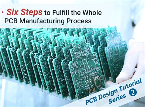
Aluminum PCB Manufacturing Process
The aluminum PCB manufacturing process consists of several key steps, each requiring precision and attention to detail. Let’s explore these steps in more detail.
Step 1: Substrate Preparation
The first step in aluminum PCB manufacturing is preparing the aluminum substrate. The substrate is typically an aluminum alloy, such as 5052 or 6061, chosen for its specific properties and suitability for the intended application.
The aluminum substrate is cleaned and degreased to remove any contaminants that may interfere with the subsequent processing steps. This is usually done using a combination of chemical and mechanical cleaning methods, such as alkaline cleaning, acid etching, and mechanical brushing.
After cleaning, the aluminum substrate is often anodized to create a thin, insulating layer of aluminum oxide on the surface. This anodic oxide layer provides electrical insulation and improves adhesion between the aluminum and the subsequent layers.
Step 2: Applying the Dielectric Layer
The next step is to apply a dielectric layer to the anodized aluminum substrate. The dielectric layer is an insulating material that separates the conductive copper traces from the aluminum base, preventing short circuits and signal interference.
There are several methods for applying the dielectric layer, including:
- Lamination: A prepreg (pre-impregnated) dielectric material, such as polyimide or epoxy, is laminated onto the aluminum substrate under heat and pressure.
- Coating: A liquid dielectric material, such as a polyimide or epoxy resin, is coated onto the aluminum substrate using techniques like screen printing, curtain coating, or spin coating.
- Sputtering: A thin layer of ceramic material, such as aluminum nitride or aluminum oxide, is deposited onto the aluminum substrate using a physical vapor deposition (PVD) process called sputtering.
The choice of dielectric material and application method depends on the specific requirements of the PCB, such as the desired thickness, thermal conductivity, and electrical properties.
Step 3: Creating the Conductive Pattern
Once the dielectric layer is in place, the next step is to create the conductive copper pattern on the PCB. This is typically done using a subtractive process, where a thin layer of copper is first applied to the entire surface of the dielectric layer, and then selectively removed to create the desired circuit pattern.
The copper layer is usually applied using one of two methods:
- Electroless plating: A thin layer of copper is deposited onto the dielectric surface through a chemical reduction process, without the use of an external electrical current.
- Electroplating: A thicker layer of copper is deposited onto the electroless copper layer using an electrical current in an electrolytic bath.
After the copper layer is applied, the circuit pattern is created using a photolithography process:
- A photoresist (light-sensitive polymer) is applied to the copper surface.
- The photoresist is exposed to UV light through a photomask, which contains the desired circuit pattern. The exposed areas of the photoresist become soluble in a developer solution.
- The exposed photoresist is removed using the developer solution, leaving the circuit pattern protected by the remaining photoresist.
- The unprotected copper is etched away using a chemical etching solution, typically containing cupric chloride or ferric chloride.
- The remaining photoresist is stripped away, leaving the final copper circuit pattern on the dielectric layer.
Step 4: Drilling and Plating Through Holes
Many PCBs require electrical connections between different layers of the board, which is achieved through plated through holes (PTHs). These holes are drilled through the PCB using high-speed, computer-controlled drilling machines.
After drilling, the holes are plated with copper to create an electrical connection between the layers. This is done using an electroplating process similar to the one used for creating the conductive pattern. A thin layer of electroless copper is first deposited onto the hole walls, followed by a thicker layer of electroplated copper.
Step 5: Solder Mask Application
A solder mask is a protective layer applied to the PCB to prevent accidental short circuits and improve the board’s durability. The solder mask is typically a green or other colored polymer that covers the copper traces, leaving only the exposed pads and holes where components will be soldered.
The solder mask is applied using a screen printing or photoimaging process, similar to the photolithography process used for creating the conductive pattern. The solder mask material is applied to the board, exposed to UV light through a photomask, and then developed to remove the unexposed areas.
Step 6: Surface Finish Application
The final step in the aluminum PCB manufacturing process is applying a surface finish to the exposed copper pads and holes. The surface finish protects the copper from oxidation and improves the solderability of the board.
Some common surface finishes used in aluminum PCBs include:
- HASL (Hot Air Solder Leveling): A tin-lead alloy is applied to the copper surfaces using a hot air leveling process.
- ENIG (Electroless Nickel Immersion Gold): A thin layer of electroless nickel is deposited onto the copper, followed by a thin layer of immersion gold.
- OSP (Organic Solderability Preservative): A thin, organic coating is applied to the copper surfaces to protect them from oxidation.
After the surface finish is applied, the aluminum PCB is ready for final inspection and testing before being shipped to the customer.

Advantages of Aluminum PCBs in PCB Manufacturing
Aluminum PCBs offer several advantages over traditional FR-4 PCBs in the manufacturing process:
- Faster heat dissipation: The high thermal conductivity of aluminum allows for faster heat dissipation during the manufacturing process, reducing the risk of thermal damage to the board and components.
- Improved dimensional stability: Aluminum has a lower coefficient of thermal expansion (CTE) than FR-4, meaning it is less likely to warp or deform during the manufacturing process, resulting in higher yields and fewer defects.
- Better high-frequency performance: Aluminum provides better shielding against electromagnetic interference (EMI) and has lower dielectric losses than FR-4, making it ideal for high-frequency applications.
- Enhanced mechanical strength: Aluminum is stronger and more durable than FR-4, providing better resistance to vibration and shock during the manufacturing process and in the final application.

Quality Control in Aluminum PCB Manufacturing
Quality control is critical in aluminum PCB manufacturing to ensure that the final product meets the required specifications and performs reliably in the intended application. Some key quality control measures include:
- Incoming material inspection: All incoming materials, including the aluminum substrate, dielectric materials, and copper foils, are inspected for quality and conformance to specifications.
- In-process inspection: Various inspections are carried out at different stages of the manufacturing process, such as after the dielectric layer application, copper pattern creation, and solder mask application, to identify and correct any defects or deviations from the specifications.
- Electrical testing: The finished PCBs are subjected to electrical tests, such as continuity, insulation resistance, and high-potential (hipot) tests, to ensure that the board functions as intended and meets the required electrical specifications.
- Visual inspection: The PCBs are visually inspected for any surface defects, such as scratches, pinholes, or contamination, using automated optical inspection (AOI) systems or manual inspection under magnification.
- Dimensional inspection: The PCBs are measured using coordinate measuring machines (CMMs) or other metrology tools to ensure that they meet the required dimensional tolerances.
By implementing strict quality control measures throughout the manufacturing process, PCB factories can ensure that the aluminum PCBs they produce are of the highest quality and reliability.
Frequently Asked Questions (FAQ)
-
How do aluminum PCBs differ from traditional FR-4 PCBs?
Aluminum PCBs use an aluminum substrate instead of the glass-reinforced epoxy laminate (FR-4) used in traditional PCBs. This provides better thermal conductivity, mechanical strength, and high-frequency performance compared to FR-4 PCBs. -
What are the main applications for aluminum PCBs?
Aluminum PCBs are commonly used in applications that require high power dissipation, such as LED lighting, power electronics, and automotive systems. They are also used in high-frequency applications, such as RF and microwave circuits, due to their better EMI shielding and lower dielectric losses. -
What are the key steps in the aluminum PCB manufacturing process?
The main steps in aluminum PCB manufacturing include substrate preparation, dielectric layer application, conductive pattern creation, drilling and plating through holes, solder mask application, and surface finish application. -
What quality control measures are used in aluminum PCB manufacturing?
Quality control measures in aluminum PCB manufacturing include incoming material inspection, in-process inspection at various stages, electrical testing, visual inspection, and dimensional inspection using automated systems and metrology tools. -
What are the advantages of using aluminum PCBs in the manufacturing process?
Aluminum PCBs offer faster heat dissipation, improved dimensional stability, better high-frequency performance, and enhanced mechanical strength compared to FR-4 PCBs during the manufacturing process. This results in higher yields, fewer defects, and more reliable final products.
Conclusion
Aluminum PCBs are a valuable alternative to traditional FR-4 PCBs in applications that require high thermal conductivity, mechanical strength, and high-frequency performance. The aluminum PCB manufacturing process involves several key steps, including substrate preparation, dielectric layer application, conductive pattern creation, drilling and plating through holes, solder mask application, and surface finish application.
By understanding the advantages of aluminum PCBs and the intricacies of the manufacturing process, PCB Designers and engineers can make informed decisions when selecting the most suitable substrate material for their applications. Furthermore, by implementing strict quality control measures throughout the manufacturing process, PCB factories can ensure that the aluminum PCBs they produce are of the highest quality and reliability, meeting the demanding requirements of today’s electronics industry.
As technology continues to advance and the demand for high-performance, reliable electronics grows, aluminum PCBs are poised to play an increasingly important role in the PCB manufacturing landscape.


Leave a Reply