Introduction to Flexible PCBs
Flexible printed circuit boards (PCBs) have gained significant popularity in recent years due to their versatility, reliability, and ability to fit into compact spaces. These PCBs are made from flexible materials, such as polyimide or polyester, allowing them to bend, twist, and fold without losing their electrical integrity. Flexible PCBs find applications in various industries, including consumer electronics, medical devices, automotive, aerospace, and more.
What are Flexible PCBs?
Flexible PCBs, also known as flex circuits or flexible printed circuits (FPCs), are a type of printed circuit board that uses flexible base materials instead of rigid substrates like FR-4. The conductive traces are printed on the flexible substrate, enabling the PCB to bend and conform to various shapes and sizes.
Advantages of Flexible PCBs
Flexible PCBs offer several advantages over traditional rigid PCBs:
- Space-saving: Flexible PCBs can be folded, bent, or twisted to fit into tight spaces, making them ideal for compact electronic devices.
- Weight reduction: The thin and lightweight nature of flexible PCBs helps reduce the overall weight of the end product.
- Improved reliability: Flexible PCBs can withstand vibrations, shocks, and extreme temperatures better than rigid PCBs, enhancing their reliability.
- Enhanced electrical performance: The shorter interconnects and reduced capacitance in flexible PCBs lead to improved electrical performance and signal integrity.
- Design flexibility: Flexible PCBs allow for creative and innovative product designs that would be challenging to achieve with rigid PCBs.
Flexible PCB Manufacturing Process
The manufacturing process of flexible PCBs involves several steps, each requiring precise control and expertise. The following sections outline the key stages in flexible PCB manufacturing.
1. Substrate Selection
The first step in flexible PCB manufacturing is selecting the appropriate substrate material. The most common substrates used are:
- Polyimide (PI): Known for its excellent thermal stability, chemical resistance, and mechanical strength.
- Polyester (PET): Offers good electrical properties and is cost-effective for less demanding applications.
The substrate thickness typically ranges from 25 to 125 microns (μm).
2. Copper Cladding
The selected substrate is then laminated with a thin layer of copper on one or both sides. The copper thickness can vary from 9 to 70 μm, depending on the application requirements. The copper-clad substrate is then cleaned and prepared for the subsequent processes.
3. Imaging and Etching
The desired circuit pattern is transferred onto the copper-clad substrate using photolithography. A photoresist layer is applied, exposed to UV light through a photomask, and developed to create the circuit pattern. The exposed copper is then etched away using a chemical solution, leaving behind the desired conductive traces.
4. Coverlay Application
To protect the circuitry and provide insulation, a coverlay is laminated onto the etched substrate. The coverlay is typically made of polyimide or polyester and has adhesive on one side. Openings for component mounting and interconnections are created in the coverlay using laser cutting or punching.
5. Surface Finish
To enhance solderability and protect the exposed copper traces, a surface finish is applied. Common surface finishes for flexible PCBs include:
- ENIG (Electroless Nickel Immersion Gold)
- ENEPIG (Electroless Nickel Electroless Palladium Immersion Gold)
- OSP (Organic Solderability Preservative)
- Immersion Silver
- Immersion Tin
6. Cutting and Singulation
The final step in flexible PCB manufacturing is cutting and singulating the individual circuits from the panel. This is typically done using a laser cutter or a die-cutting machine, ensuring precise and clean edges.

Flexible PCB Assembly
Once the flexible PCBs are manufactured, they undergo the assembly process to mount electronic components and create functional circuits. The assembly process for flexible PCBs is similar to that of rigid PCBs, with a few additional considerations.
1. Solder Paste Application
Solder paste is applied to the component pads on the flexible PCB using a stencil printing process. The stencil ensures precise and consistent solder paste deposition. Due to the flexible nature of the substrate, additional support may be required during stencil printing to maintain accuracy.
2. Component Placement
Surface mount components are placed onto the solder paste deposits using pick-and-place machines. The machines use vision systems to accurately position the components on the pads. Flexible PCBs may require specialized fixturing to keep the substrate flat and stable during component placement.
3. Reflow Soldering
The assembled flexible PCB is then subjected to a reflow soldering process, where the solder paste is melted to create electrical and mechanical connections between the components and the PCB. Reflow soldering for flexible PCBs requires careful control of the temperature profile to avoid damaging the substrate or components.
4. Inspection and Testing
After reflow soldering, the assembled flexible PCBs undergo visual inspection and electrical testing to ensure proper functionality and quality. Automated optical inspection (AOI) systems and flying probe testers are commonly used for this purpose.

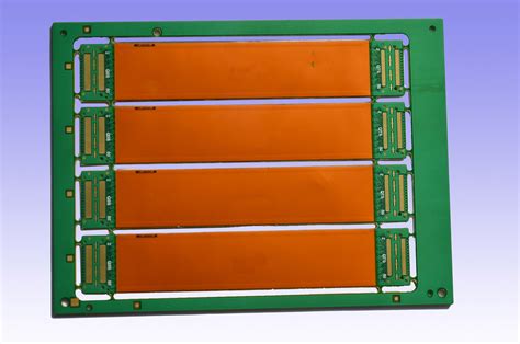
Multi-Layer Flexible PCBs
Flexible PCBs can be manufactured with multiple layers to accommodate more complex circuitry and higher component density. Multi-layer flexible PCBs are constructed by laminating several single-layer flexible circuits together with insulating adhesive layers in between.
Types of Multi-Layer Flexible PCBs
-
Double-sided flexible PCBs: These PCBs have conductive traces on both sides of the substrate, allowing for higher component density and more complex routing.
-
Multi-layer flexible PCBs: These PCBs consist of three or more conductive layers separated by insulating layers. They offer the highest level of design flexibility and circuit density.
-
Rigid-Flex PCBs: These hybrid PCBs combine rigid and flexible sections, enabling the integration of both types of circuits into a single board. The rigid sections provide mechanical support and allow for the mounting of larger components, while the flexible sections offer the benefits of flex circuits.
Considerations for Multi-Layer Flexible PCBs
When designing and manufacturing multi-layer flexible PCBs, several factors need to be considered:
-
Layer stack-up: The arrangement of conductive and insulating layers should be carefully planned to ensure proper signal integrity and impedance control.
-
Adhesive selection: The choice of adhesive for laminating the layers is crucial, as it affects the flexibility, reliability, and performance of the final product.
-
Via design: Vias in multi-layer flexible PCBs require special attention to ensure reliable interconnections between layers without compromising flexibility.
-
Bend radius: The minimum bend radius of the multi-layer flexible PCB should be determined based on the number of layers, substrate thickness, and material properties to avoid stress and damage during flexing.

Applications of Flexible PCBs
Flexible PCBs find applications in a wide range of industries and products. Some common applications include:
- Consumer electronics: Smartphones, wearables, digital cameras, and gaming devices.
- Medical devices: Implantable devices, diagnostic equipment, and patient monitoring systems.
- Automotive: In-vehicle infotainment systems, sensors, and electronic control units (ECUs).
- Aerospace: Avionics, satellites, and missile systems.
- Industrial: Robotics, automation, and process control equipment.
Frequently Asked Questions (FAQ)
1. What is the minimum bend radius for flexible PCBs?
The minimum bend radius depends on the substrate material, thickness, and the number of layers in the flexible PCB. As a general rule, the minimum bend radius is 6 times the total thickness of the PCB. However, it is essential to consult with the PCB manufacturer and adhere to their guidelines for specific requirements.
2. Can flexible PCBs be reworked or repaired?
Yes, flexible PCBs can be reworked or repaired, but it requires specialized skills and equipment. Rework and repair processes should be performed by experienced technicians to avoid damaging the delicate substrate or components. It is essential to follow the manufacturer’s guidelines and use appropriate tools and techniques.
3. How do I choose the right surface finish for my flexible PCB?
The choice of surface finish depends on several factors, such as the application environment, solderability requirements, shelf life, and cost. ENIG and ENEPIG are popular choices for their excellent solderability and durability. OSP is a cost-effective option for shorter shelf life requirements. Immersion silver and tin offer good solderability but may have limitations in terms of shelf life and environmental resistance.
4. Can flexible PCBs be used in high-temperature applications?
Yes, flexible PCBs can be designed to withstand high temperatures. Polyimide (PI) substrates are commonly used for high-temperature applications due to their excellent thermal stability. They can typically withstand temperatures up to 200°C or higher. However, the temperature rating of the components and the solder joints should also be considered when designing flexible PCBs for high-temperature applications.
5. What are the challenges in manufacturing multi-layer flexible PCBs?
Manufacturing multi-layer flexible PCBs presents several challenges, including:
1. Maintaining precise alignment between layers during lamination
2. Ensuring reliable interlayer connections through vias
3. Controlling the adhesive flow and thickness between layers
4. Managing the increased complexity in design and layout
5. Handling and processing the delicate multi-layer structures
To overcome these challenges, manufacturers use advanced equipment, specialized processes, and strict quality control measures. Close collaboration between the design team and the manufacturing team is essential to ensure the successful production of multi-layer flexible PCBs.
Conclusion
Flexible PCBs have become an essential part of modern electronics, offering numerous advantages over traditional rigid PCBs. The manufacturing and assembly processes for flexible PCBs require specialized knowledge, equipment, and techniques to ensure high-quality and reliable end products.
From single-layer to multi-layer designs, flexible PCBs can be customized to meet the specific requirements of various applications across different industries. As technology continues to advance, the demand for flexible PCBs is expected to grow, driving innovations in materials, manufacturing processes, and assembly techniques.
By understanding the fundamentals of flexible PCB manufacturing and assembly, designers and engineers can create innovative and reliable electronic products that leverage the benefits of this versatile technology.
| Layer Count | Typical Applications | Advantages | Disadvantages |
|---|---|---|---|
| 1 | Simple circuits, low-cost products | Cost-effective, easy to manufacture | Limited routing and component density |
| 2 (Double-sided) | Moderate complexity circuits, consumer electronics | Higher component density, more routing options | Increased manufacturing complexity and cost |
| 3-4 | Complex circuits, medical devices, automotive | High component density, enhanced signal integrity | Higher cost, more challenging to manufacture |
| 5-8 | Very complex circuits, aerospace, defense | Highest component density, improved performance | Very high cost, specialized manufacturing processes |
| 9-10 | Extremely complex circuits, niche applications | Maximum design flexibility and performance | Extremely high cost, limited manufacturers capable of production |


Leave a Reply