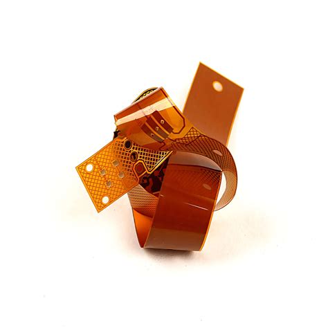
What is a Flexible PCB?
A flexible PCB, also known as a flex circuit or flexible printed wiring board (PWB), is a type of printed circuit board that consists of a thin, flexible substrate with conductive traces and components mounted on it. Unlike rigid PCBs, which are made from a solid, inflexible material such as fiberglass or epoxy resin, flexible PCBs are constructed using a pliable substrate material, typically polyimide or polyester film.
The flexibility of these PCBs allows them to conform to various shapes and contours, making them ideal for applications where space is limited or where the circuit needs to bend or flex during operation. Flexible PCBs can be single-sided, double-sided, or multilayer, depending on the complexity of the circuit design and the number of interconnections required.
Advantages of Flexible PCBs
Flexible PCBs offer several key advantages over their rigid counterparts:
-
Flexibility and Conformability: The most obvious benefit of flexible PCBs is their ability to bend, twist, and conform to various shapes and contours. This enables designers to create more compact and space-efficient electronic devices, as the flexible circuit can be folded or wrapped around components or integrated into tight spaces.
-
Reduced Weight and Thickness: Flexible PCBs are typically thinner and lighter than rigid PCBs, as they do not require the same level of structural support. This makes them particularly well-suited for applications where weight and size are critical factors, such as in aerospace, automotive, and wearable electronics.
-
Increased Durability and Reliability: The flexible nature of these PCBs allows them to withstand repeated bending and flexing without cracking or breaking, making them more durable than rigid PCBs in dynamic environments. Additionally, the absence of connectors and wires between separate rigid boards reduces the potential for connection failures, improving overall system reliability.
-
Improved Signal Integrity: Flexible PCBs can offer better signal integrity compared to rigid PCBs with connectors and cables. The continuous traces on a flexible PCB eliminate the need for multiple connectors and wires, reducing signal reflections, crosstalk, and electromagnetic interference (EMI).
-
Cost-Effective for High-Volume Production: While the initial design and setup costs for flexible PCBs may be higher than those for rigid PCBs, they can be more cost-effective in high-volume production runs. This is due to the reduced assembly time and the elimination of connectors and wires, which can simplify the manufacturing process.

Flexible PCB Manufacturing Process
The manufacturing process for flexible PCBs shares many similarities with that of rigid PCBs, but with some unique considerations and techniques to accommodate the flexible substrate material. The following steps outline the typical flexible PCB manufacturing process:
-
Design and Layout: The first step in the manufacturing process is to design the circuit layout using computer-aided design (CAD) software. The designer must consider the specific requirements of the flexible PCB, such as bend radius, material selection, and component placement, to ensure optimal performance and reliability.
-
Material Selection: The choice of substrate material is critical in flexible PCB manufacturing. Polyimide is the most commonly used substrate due to its excellent thermal stability, chemical resistance, and mechanical properties. Other materials, such as polyester or liquid crystal polymer (LCP), may be used for specific applications or cost considerations.
-
Substrate Preparation: The selected substrate material is cut to the desired size and shape using precision cutting tools. The substrate may also undergo a cleaning process to remove any contaminants or debris that could affect the adhesion of the conductive layers.
-
Copper Lamination: A thin layer of copper foil is laminated onto the prepared substrate using heat and pressure. The copper foil can be pre-treated with an adhesive or bonded directly to the substrate material, depending on the specific manufacturing process and requirements.
-
Patterning and Etching: The desired circuit pattern is transferred onto the copper-clad substrate using a photolithography process. A photoresist layer is applied to the copper surface, and the circuit pattern is exposed using UV light through a photomask. The exposed areas of the photoresist are then developed and removed, leaving the desired circuit pattern protected by the remaining photoresist. The exposed copper is etched away using a chemical solution, leaving only the desired conductive traces.
-
Via Formation: Vias are tiny holes drilled through the substrate and copper layers to interconnect different layers of the flexible PCB. Various methods can be used to create vias, such as mechanical drilling, laser drilling, or photovia formation, depending on the size and density of the vias required.
-
Coverlay Application: A coverlay, which is a thin insulating layer, is applied over the etched circuit pattern to protect the conductive traces and provide electrical insulation. The coverlay is typically made from the same material as the substrate and is laminated using heat and pressure.
-
Surface Finish: To enhance the durability and solderability of the exposed copper traces and pads, a surface finish is applied. Common surface finishes include hot air solder leveling (HASL), electroless nickel immersion gold (ENIG), and immersion silver.
-
Solder Mask Application: A solder mask is a thin, protective layer applied over the coverlay and exposed copper areas to prevent solder bridging and provide additional insulation. The solder mask is typically applied using a screen printing or photoimaging process and is available in various colors for easy identification and aesthetics.
-
Component Assembly: Finally, the electronic components are assembled onto the flexible PCB using various techniques, such as surface mount technology (SMT), chip-on-flex (COF), or flip-chip bonding. The assembLED PCB undergoes a reflow soldering process to establish electrical connections between the components and the conductive traces.
-
Testing and Inspection: The completed flexible PCB undergoes rigorous testing and inspection to ensure proper functionality, reliability, and compliance with industry standards. This may include electrical continuity tests, insulation resistance tests, and visual inspections for defects or anomalies.

Applications of Flexible PCBs
Flexible PCBs find applications in a wide range of industries and products, thanks to their unique properties and advantages. Some common applications include:
-
Consumer Electronics: Flexible PCBs are widely used in smartphones, tablets, laptops, and wearable devices, where space constraints and the need for compact, lightweight designs are paramount. They enable the integration of various components, such as displays, sensors, and batteries, into slim and ergonomic form factors.
-
Medical Devices: The biocompatibility and flexibility of certain substrate materials make flexible PCBs well-suited for medical applications, such as implantable devices, diagnostic equipment, and patient monitoring systems. Flexible PCBs can conform to the contours of the human body and withstand the stresses of implantation and long-term use.
-
Automotive Electronics: The harsh environmental conditions and vibrations experienced in automotive applications demand robust and reliable electronic systems. Flexible PCBs are used in various automotive electronics, such as dashboard displays, sensor systems, and engine control modules, where their flexibility and durability provide essential benefits.
-
Aerospace and Defense: In aerospace and defense applications, where weight reduction and reliability are critical, flexible PCBs offer significant advantages. They are used in avionics systems, satellite components, and military equipment, where their ability to conform to complex shapes and withstand extreme conditions is highly valued.
-
Industrial Automation: Flexible PCBs are increasingly used in industrial automation systems, such as robotics, motor controls, and sensor networks. Their flexibility allows for more efficient cable management and reduces the risk of connection failures in moving or vibrating parts.

Frequently Asked Questions (FAQ)
-
Q: What is the difference between a flexible PCB and a rigid PCB?
A: A flexible PCB is made from a thin, pliable substrate material that allows it to bend and conform to various shapes, while a rigid PCB is made from a solid, inflexible material such as fiberglass or epoxy resin. Flexible PCBs offer advantages in terms of flexibility, weight reduction, and durability, while rigid PCBs provide better structural support and are suitable for applications where flexibility is not required. -
Q: What materials are commonly used for flexible PCB substrates?
A: The most commonly used substrate material for flexible PCBs is polyimide, which offers excellent thermal stability, chemical resistance, and mechanical properties. Other materials, such as polyester or liquid crystal polymer (LCP), may be used for specific applications or cost considerations. -
Q: Can flexible PCBs be multilayered?
A: Yes, flexible PCBs can be single-sided, double-sided, or multilayered, depending on the complexity of the circuit design and the number of interconnections required. Multilayer flexible PCBs allow for higher component density and more complex routing, but they also increase the manufacturing complexity and cost. -
Q: How do flexible PCBs improve signal integrity compared to rigid PCBs?
A: Flexible PCBs can offer better signal integrity compared to rigid PCBs with connectors and cables. The continuous traces on a flexible PCB eliminate the need for multiple connectors and wires, reducing signal reflections, crosstalk, and electromagnetic interference (EMI). This is particularly important in high-speed or high-frequency applications where signal integrity is critical. -
Q: What are the challenges associated with manufacturing flexible PCBs?
A: Manufacturing flexible PCBs presents some unique challenges compared to rigid PCBs. These include the need for specialized tooling and processes to handle the flexible substrate material, the difficulty in achieving fine-pitch traces and components, and the potential for delamination or cracking due to the stresses induced by bending and flexing. Careful design, material selection, and process control are essential to ensure the reliability and performance of flexible PCBs.
| Characteristic | Flexible PCB | Rigid PCB |
|---|---|---|
| Substrate Material | Polyimide, Polyester, LCP | FR-4, Ceramic, Aluminum |
| Flexibility | High | Low |
| Weight | Low | High |
| Thickness | Thin (typically 0.1-0.3 mm) | Thick (typically 0.6-2.0 mm) |
| Durability | High (withstands bending and flexing) | Low (prone to cracking under stress) |
| Signal Integrity | High (continuous traces, fewer connectors) | Moderate (connectors and cables can degrade signal) |
| Component Density | Moderate to High | High |
| Cost | Higher (specialized materials and processes) | Lower (standard materials and processes) |
In conclusion, flexible PCBs offer a versatile and reliable solution for interconnecting electronic components in a wide range of applications where flexibility, weight reduction, and durability are essential. The unique properties of flexible PCBs, combined with advancements in materials and manufacturing processes, have enabled the development of increasingly complex and compact electronic devices across various industries. As the demand for wearable, implantable, and space-constrained electronics continues to grow, the importance of flexible PCBs in shaping the future of electronics cannot be overstated.


Leave a Reply