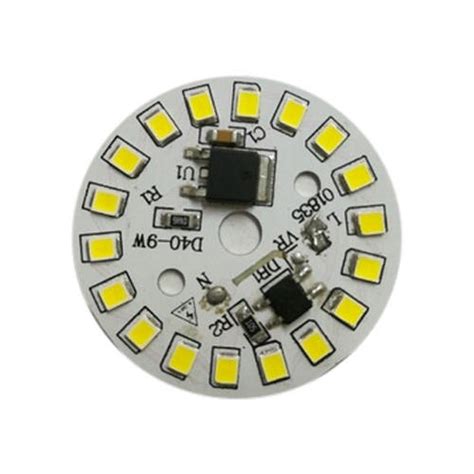
Introduction to LED PCB
Light-emitting diode (LED) technology has revolutionized the lighting industry, offering energy-efficient, long-lasting, and versatile solutions for various applications. At the heart of every LED light fixture lies a printed circuit board (PCB) that serves as the foundation for the electrical and mechanical components. In this comprehensive article, we will delve into the world of LED PCB fabrication and assembly, exploring the key aspects, best practices, and expert insights to help you navigate this exciting field.
The Importance of LED PCB Design
Thermal Management Considerations
One of the most critical aspects of LED PCB design is thermal management. LEDs generate heat during operation, and if not properly dissipated, this heat can lead to reduced performance, shortened lifespan, and even failure. When designing an LED PCB, it is essential to incorporate effective thermal management techniques, such as:
- Using high-quality, thermally conductive PCB materials like aluminum or copper-clad laminates
- Incorporating thermal vias to transfer heat from the LED to the PCB’s heat sink
- Designing adequate copper pour and trace widths to facilitate heat dissipation
- Utilizing thermal interface materials (TIMs) between the LED and the PCB to enhance heat transfer
Electrical Design Best Practices
In addition to thermal management, electrical design plays a vital role in ensuring the optimal performance and reliability of LED PCBs. Some key considerations include:
- Selecting appropriate LED drivers and power supplies to ensure stable current and voltage
- Designing proper trace routing and spacing to minimize electromagnetic interference (EMI) and signal integrity issues
- Implementing appropriate circuit protection measures, such as fuses and transient voltage suppressors (TVS), to safeguard against electrical overstress
- Utilizing high-quality components and connectors to ensure reliable electrical connections and minimize power losses
Optical Design Considerations
The optical design of an LED PCB is crucial for achieving the desired light output, distribution, and quality. Some factors to consider include:
- Choosing the appropriate LED type, color temperature, and binning to meet the application requirements
- Designing reflectors, lenses, and diffusers to control the light beam angle, intensity, and uniformity
- Optimizing the LED placement and spacing to achieve uniform illumination and minimize shadowing effects
- Considering the impact of PCB surface finish on light reflection and absorption

LED PCB Fabrication Process
PCB Material Selection
The choice of PCB material is critical for LED applications, as it directly impacts the thermal, electrical, and mechanical performance of the final product. Some popular options include:
- FR-4: A cost-effective, glass-reinforced epoxy laminate suitable for general-purpose LED applications
- Metal Core PCB (MCPCB): A PCB with a metal core, typically aluminum, that offers excellent thermal conductivity for high-power LED applications
- Ceramic PCB: A high-performance, thermally stable substrate ideal for harsh environments and high-temperature applications
- Flexible PCB: A thin, flexible substrate that enables unique form factors and applications, such as wearable electronics and automotive lighting
PCB Manufacturing Steps
The LED PCB fabrication process involves several key steps, including:
- PCB Design and Layout: Creating the schematic and layout files using electronic design automation (EDA) software
- PCB Fabrication: Manufacturing the bare PCB through processes like etching, drilling, and plating
- Solder Mask Application: Applying a protective layer to the PCB to prevent short circuits and improve solderability
- Silkscreen Printing: Adding text, logos, and component designators to the PCB for easy identification and assembly
- Surface Finish: Applying a final finish, such as HASL, ENIG, or OSP, to protect the exposed copper and enhance solderability
Quality Control and Testing
To ensure the highest quality and reliability of LED PCBs, rigorous quality control and testing procedures are essential. Some common techniques include:
- Visual inspection: Checking for defects, such as scratches, dents, or discoloration
- Automated optical inspection (AOI): Using machine vision systems to detect manufacturing defects and component placement errors
- X-ray inspection: Examining the internal structure of the PCB for hidden defects, such as voids or delamination
- Electrical testing: Verifying the electrical functionality and performance of the PCB, including continuity, insulation resistance, and high-potential testing
- Thermal testing: Evaluating the thermal performance of the PCB under various operating conditions to ensure proper heat dissipation and reliability

LED PCB Assembly Process
Component Selection and Procurement
Choosing the right components for an LED PCB assembly is crucial for achieving the desired performance, reliability, and cost-effectiveness. Some key factors to consider when selecting components include:
- LED specifications: Luminous flux, forward voltage, color temperature, and viewing angle
- Driver and power supply requirements: Current and voltage ratings, dimming capabilities, and efficiency
- Passive components: Resistors, capacitors, and inductors with appropriate ratings and tolerances
- Connectors and fasteners: Robust and reliable options that meet the mechanical and environmental requirements
When procuring components, it is essential to work with reputable suppliers and ensure proper documentation, such as datasheets, certificates of conformance, and RoHS compliance.
SMT and THT Assembly Techniques
LED PCB assembly typically involves a combination of surface mount technology (SMT) and through-hole technology (THT) processes. SMT is the most common method for mounting smaller components, such as LED packages and passive components, while THT is used for larger components or those requiring higher mechanical strength, such as connectors and heat sinks.
The SMT assembly process includes the following steps:
1. Solder Paste Application: Depositing solder paste onto the PCB pads using techniques like stencil printing or dispensing
2. Component Placement: Placing the SMT components onto the solder paste using pick-and-place machines or manual methods
3. Reflow Soldering: Heating the PCB assembly in a reflow oven to melt the solder paste and form reliable electrical and mechanical connections
The THT assembly process involves the following steps:
1. Component Insertion: Inserting the THT components into the designated through-holes on the PCB
2. Wave Soldering: Passing the PCB assembly through a molten solder wave to form the solder joints on the bottom side of the board
3. Manual Soldering: Hand-soldering specific components or making repairs using a soldering iron
Inspection and Testing
After the LED PCB assembly process, thorough inspection and testing are necessary to ensure the quality and functionality of the final product. Some standard inspection and testing methods include:
- Visual inspection: Checking for component placement accuracy, solder joint quality, and overall workmanship
- Automated optical inspection (AOI): Using machine vision systems to detect assembly defects and component orientation errors
- X-ray inspection: Examining the internal structure of the solder joints for hidden defects, such as voids or bridging
- In-circuit testing (ICT): Verifying the electrical functionality and performance of the assembled PCB using dedicated test fixtures and software
- Functional testing: Evaluating the overall performance of the LED PCB assembly under real-world operating conditions, including light output, color consistency, and thermal management

Advanced LED PCB Technologies
Flexible and Stretchable LED PCBs
Flexible and stretchable LED PCBs are gaining popularity in applications that require conformable or wearable lighting solutions. These PCBs use flexible substrates, such as polyimide or thermoplastic polyurethane (TPU), and stretchable conductive materials, like silver nanowires or conductive polymers, to enable bending, folding, and stretching without compromising electrical performance.
Some key applications for flexible and stretchable LED PCBs include:
– Wearable electronics: Smart clothing, fitness trackers, and medical devices
– Automotive lighting: Conformable interior and exterior lighting, such as dashboard displays and tail lights
– Architectural lighting: Curved or irregular-shaped lighting fixtures and installations
– Soft robotics: Deformable and adaptable lighting for robotic applications
COB and CSP LED Packaging
Chip-on-board (COB) and chip-scale package (CSP) are advanced LED packaging technologies that offer improved performance, reliability, and miniaturization compared to traditional LED packages.
COB LEDs involve directly mounting the bare LED chips onto the PCB substrate and encapsulating them with a phosphor coating and lens. This approach eliminates the need for individual packaging and enables higher packing density, better thermal management, and improved color consistency.
CSP LEDs, on the other hand, use a miniaturized package that is only slightly larger than the LED chip itself. This compact design allows for higher-resolution displays, improved beam control, and reduced package-related optical losses.
Both COB and CSP LED technologies are widely used in applications such as:
– High-power lighting: Spot lights, flood lights, and high-bay luminaires
– Display backlighting: LCD and OLED displays for smartphones, tablets, and televisions
– Horticulture lighting: Grow lights and vertical farming systems
– Automotive lighting: Headlights, daytime running lights, and interior lighting
Smart LED PCB Solutions
The integration of intelligence and connectivity into LED PCBs is driving the development of smart lighting solutions. By incorporating sensors, microcontrollers, and wireless communication modules, smart LED PCBs enable advanced features such as:
- Remote control and monitoring: Adjusting brightness, color temperature, and scheduling via smartphone apps or web interfaces
- Occupancy and daylight sensing: Automatically adjusting the light output based on the presence of people or ambient light levels
- Predictive maintenance: Monitoring the health and performance of the LED PCB and providing alerts for proactive maintenance
- Energy optimization: Implementing intelligent control strategies to minimize energy consumption and maximize efficiency
Some common communication protocols used in smart LED PCB solutions include:
– Zigbee: A low-power, mesh networking protocol for building automation and IoT applications
– Bluetooth Low Energy (BLE): A short-range, low-power wireless communication standard for mobile devices and wearables
– Wi-Fi: A high-speed, long-range wireless networking protocol for internet connectivity and cloud-based services
LED PCB FAQs
Q1: What are the benefits of using LED PCBs compared to traditional lighting solutions?
A1: LED PCBs offer several advantages over traditional lighting solutions, including:
– Higher energy efficiency and lower power consumption
– Longer lifespan and reduced maintenance costs
– Compact size and design flexibility
– Instant start-up and dimming capabilities
– Environmentally friendly, with no mercury or other hazardous materials
Q2: How do I choose the right LED PCB material for my application?
A2: The choice of LED PCB material depends on several factors, such as:
– Thermal management requirements: Use MCPCB or ceramic PCBs for high-power applications
– Mechanical requirements: Use flexible or rigid PCBs based on the application’s form factor and durability needs
– Environmental conditions: Consider the operating temperature, humidity, and chemical exposure when selecting the material
– Cost and volume: Evaluate the trade-offs between performance and cost for your specific production scale
Q3: What are the key considerations for LED PCB thermal management?
A3: Effective thermal management is crucial for LED PCB performance and reliability. Some key considerations include:
– Selecting high-thermal-conductivity PCB materials, such as MCPCB or ceramic
– Designing adequate copper pour and trace widths to facilitate heat dissipation
– Incorporating thermal vias and heat sinks to transfer heat away from the LEDs
– Using thermal interface materials (TIMs) to enhance heat transfer between the LED and PCB
– Optimizing the LED placement and spacing to minimize thermal crosstalk
Q4: How can I ensure the quality and reliability of my LED PCB assembly?
A4: To ensure the highest quality and reliability of your LED PCB assembly, follow these best practices:
– Design for manufacturability (DFM) and design for assembly (DFA) principles
– Select high-quality components from reputable suppliers
– Implement robust quality control and testing procedures, such as AOI, X-ray, and functional testing
– Work with experienced PCB fabrication and assembly partners who adhere to industry standards and certifications
– Conduct thorough validation and reliability testing, including thermal cycling, vibration, and accelerated life testing
Q5: What are some emerging trends and future directions in LED PCB technology?
A5: Some key trends and future directions in LED PCB technology include:
– Miniaturization and integration of LED packages, such as COB and CSP
– Adoption of flexible and stretchable LED PCBs for wearable and conformable applications
– Development of smart LED PCB solutions with integrated sensors, controls, and connectivity
– Emphasis on sustainable and eco-friendly LED PCB materials and manufacturing processes
– Exploration of advanced optical technologies, such as micro-optics and quantum dot LEDs, for improved light quality and efficiency
Conclusion
LED PCB fabrication and assembly is a complex and multidisciplinary field that requires a deep understanding of thermal, electrical, optical, and mechanical principles. By following best practices in design, material selection, manufacturing, and testing, you can create high-performance, reliable, and cost-effective LED PCB solutions for a wide range of applications.
As the lighting industry continues to evolve, staying up-to-date with the latest technologies, trends, and regulations is essential for success. By partnering with experienced LED PCB fabrication and assembly experts, you can navigate the challenges and opportunities in this exciting field and bring your innovative lighting ideas to life.
| LED PCB Material | Key Features | Typical Applications |
|---|---|---|
| FR-4 | Cost-effective, general-purpose | Indoor lighting, signage |
| Metal Core PCB (MCPCB) | High thermal conductivity | High-power lighting, automotive |
| Ceramic PCB | High thermal stability, durability | Harsh environments, high-temperature |
| Flexible PCB | Thin, conformable, lightweight | Wearable electronics, automotive interior |
| LED Package Type | Key Features | Typical Applications |
|---|---|---|
| Through-hole | Robust, easy to assembly | Indicators, displays |
| Surface Mount (SMD) | Compact, automated assembly | General lighting, backlighting |
| Chip-on-Board (COB) | High packing density, improved thermal management | High-power lighting, horticulture |
| Chip-Scale Package (CSP) | Miniaturized, improved optical control | High-resolution displays, automotive |


Leave a Reply