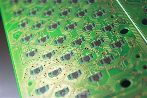
What is Carbon Ink PCB?
Carbon ink PCB is a type of printed circuit board that utilizes conductive carbon-based ink to create electronic circuits on a substrate material, such as paper or plastic. Unlike conventional PCBs that use copper traces, carbon ink PCBs employ a special formulation of carbon-based ink that exhibits excellent electrical conductivity and mechanical properties.
The concept of carbon ink PCB originated from the need for flexible, lightweight, and cost-effective electronic circuits. By replacing the traditional copper traces with carbon ink, manufacturers can achieve these desired characteristics while maintaining the functionality and reliability of the circuit.
Properties of Carbon Ink
To understand the significance of carbon ink PCB, it is essential to explore the properties of the carbon ink itself. Carbon ink is a conductive material composed of carbon nanoparticles suspended in a liquid medium, such as water or organic solvents. The key properties of carbon ink include:
- Electrical Conductivity: Carbon ink exhibits excellent electrical conductivity, allowing it to efficiently transmit electrical signals within the circuit. The conductivity of carbon ink can be tailored by adjusting the concentration and size of the carbon nanoparticles.
- Flexibility: Unlike rigid copper traces, carbon ink can be printed on flexible substrates, such as paper or plastic films. This flexibility enables the creation of bendable and conformable electronic devices, opening up new possibilities for wearable electronics and flexible displays.
- Lightweight: Carbon ink is significantly lighter than copper, resulting in PCBs with reduced overall weight. This property is particularly advantageous for applications where weight is a critical factor, such as aerospace and portable devices.
- Cost-effectiveness: The manufacturing process of carbon ink PCB is generally less expensive compared to traditional PCB Fabrication methods. The use of readily available substrates and the ability to print circuits using inkjet or screen printing techniques contribute to the cost-effectiveness of this technology.
Manufacturing Process
The manufacturing process of carbon ink PCB involves several key steps:
- Substrate Preparation: The chosen substrate, such as paper or plastic film, is cleaned and treated to ensure proper adhesion of the carbon ink. Surface treatments, such as corona discharge or plasma treatment, may be applied to enhance the ink’s bonding characteristics.
- Circuit Design: The desired electronic circuit is designed using computer-aided design (CAD) software. The design is optimized for the specific properties of carbon ink, considering factors such as trace width, spacing, and Impedance Matching.
- Printing: The carbon ink is deposited onto the substrate using various printing techniques, such as inkjet printing, screen printing, or aerosol jet printing. The choice of printing method depends on the desired resolution, speed, and scalability of the manufacturing process.
- Curing: After printing, the carbon ink is cured to remove the liquid medium and solidify the conductive traces. Curing can be achieved through heat treatment, ultraviolet (UV) exposure, or a combination of both. The curing process ensures the stability and durability of the printed circuits.
- Post-processing: Additional post-processing steps may be required, depending on the specific application. These steps can include the application of protective coatings, the attachment of electronic components, or the integration of the carbon ink PCB into a larger system.

Advantages of Carbon Ink PCB
Carbon ink PCB offers several compelling advantages over traditional PCB manufacturing methods:
- Flexibility and Conformability: The ability to print carbon ink on flexible substrates enables the creation of bendable and conformable electronic devices. This flexibility opens up new possibilities for wearable electronics, flexible displays, and sensors that can adapt to curved surfaces.
- Lightweight and Thin: Carbon ink PCBs are significantly lighter and thinner compared to their copper counterparts. This reduction in weight and thickness is particularly beneficial for applications where portability and miniaturization are essential, such as in aerospace, automotive, and consumer electronics.
- Cost-effectiveness: The manufacturing process of carbon ink PCB is generally less expensive than traditional PCB fabrication methods. The use of readily available substrates, such as paper or plastic films, and the ability to print circuits using inkjet or screen printing techniques contribute to the cost-effectiveness of this technology.
- Environmental Friendliness: Carbon ink PCBs have a lower environmental impact compared to conventional PCBs. The use of non-toxic and biodegradable substrates, such as paper, reduces electronic waste and minimizes the ecological footprint of electronic devices.
- Rapid Prototyping: The printing-based manufacturing process of carbon ink PCB enables rapid prototyping and iteration. Designers can quickly test and refine their circuit designs, accelerating the development cycle and reducing time-to-market.

Applications of Carbon Ink PCB
Carbon ink PCB Technology finds applications in various domains, including:
- Wearable Electronics: The flexibility and lightweight nature of carbon ink PCBs make them ideal for wearable devices, such as smartwatches, fitness trackers, and medical monitoring systems. These devices can conform to the contours of the human body, providing comfort and functionality.
- Internet of Things (IoT): Carbon ink PCBs can be used in IoT devices that require low-cost, flexible, and disposable sensors. Examples include smart packaging, environmental monitoring systems, and agricultural sensors.
- Automotive Industry: The automotive industry can benefit from carbon ink PCBs in applications such as flexible displays, touch sensors, and lightweight wiring harnesses. The reduced weight and increased flexibility of carbon ink PCBs contribute to fuel efficiency and design flexibility in vehicles.
- Aerospace and Defense: Carbon ink PCBs offer advantages in aerospace and defense applications where weight reduction and conformability are critical. Lightweight and flexible electronic systems can be integrated into aircraft, satellites, and military equipment, enhancing performance and reliability.
- Medical Devices: The biocompatibility and flexibility of carbon ink PCBs make them suitable for medical applications, such as implantable devices, wearable health monitors, and disposable sensors. The ability to create conformable and lightweight devices improves patient comfort and enables continuous monitoring.
Challenges and Future Developments
While carbon ink PCB technology offers numerous benefits, there are challenges and areas for future development:
- Conductivity Enhancement: Although carbon ink exhibits good electrical conductivity, it is still lower compared to copper traces. Researchers are actively working on developing carbon ink formulations with higher conductivity to improve the performance of carbon ink PCBs.
- Durability and Reliability: The long-term durability and reliability of carbon ink PCBs need to be thoroughly investigated, especially in harsh environmental conditions. Studies are being conducted to assess the stability and performance of carbon ink circuits under various stress factors, such as temperature, humidity, and mechanical strain.
- Scalability and Mass Production: While carbon ink PCB technology has shown promising results in laboratory settings, scalability and mass production remain challenges. Efforts are being made to optimize the manufacturing process, increase production throughput, and ensure consistent quality control for large-scale production.
- Integration with Other Electronic Components: The integration of carbon ink PCBs with other electronic components, such as active devices and passive components, requires further development. Researchers are exploring techniques for seamless integration, such as conductive adhesives and direct printing of components onto the carbon ink circuits.
- Standardization and Qualification: As carbon ink PCB technology gains traction, there is a need for standardization and qualification processes to ensure consistency and reliability across different manufacturers and applications. Industry standards and guidelines are being developed to establish best practices and ensure the quality of carbon ink PCBs.
Frequently Asked Questions (FAQ)
- What is the main difference between carbon ink PCB and traditional PCB?
The main difference lies in the conductive material used. Carbon ink PCB uses conductive carbon-based ink to create electronic circuits, while traditional PCB uses copper traces. Carbon ink PCBs offer flexibility, lightweight, and cost-effectiveness compared to Copper-Based PCBs. - Can carbon ink PCBs replace traditional PCBs in all applications?
While carbon ink PCBs offer several advantages, they may not be suitable for all applications. Traditional PCBs still excel in high-power and high-frequency applications where the higher conductivity of copper is essential. Carbon ink PCBs are more suitable for low-power, flexible, and cost-sensitive applications. - Are carbon ink PCBs environmentally friendly?
Yes, carbon ink PCBs have a lower environmental impact compared to traditional PCBs. The use of non-toxic and biodegradable substrates, such as paper, reduces electronic waste and minimizes the ecological footprint of electronic devices. - What are the key properties of carbon ink used in PCBs?
The key properties of carbon ink include excellent electrical conductivity, flexibility, lightweight, and cost-effectiveness. These properties make carbon ink suitable for various applications, such as wearable electronics, IoT devices, and flexible displays. - What are the potential applications of carbon ink PCB technology?
Carbon ink PCB technology finds applications in various domains, including wearable electronics, Internet of Things (IoT), automotive industry, aerospace and defense, and medical devices. The flexibility, lightweight, and cost-effectiveness of carbon ink PCBs make them attractive for these applications.
Conclusion
Carbon ink PCB technology represents a significant advancement in the field of printed electronics. By replacing traditional copper traces with conductive carbon ink, carbon ink PCBs offer several advantages, including flexibility, lightweight, cost-effectiveness, and environmental friendliness. These properties make carbon ink PCBs suitable for a wide range of applications, from wearable electronics and IoT devices to automotive and medical industries.
As research and development in carbon ink PCB technology continue, we can expect further improvements in conductivity, durability, and scalability. The potential for carbon ink PCBs to revolutionize the electronics industry is immense, enabling the creation of innovative and sustainable electronic devices.
However, it is important to recognize that carbon ink PCB technology is still evolving, and challenges remain in terms of conductivity enhancement, long-term reliability, and mass production. Ongoing research and collaboration between academia and industry are crucial to overcoming these challenges and realizing the full potential of carbon ink PCBs.
In conclusion, carbon ink PCB technology offers a promising alternative to traditional PCB manufacturing methods, bringing forth a new era of flexible, lightweight, and environmentally friendly electronics. As this technology continues to advance, it has the potential to transform various industries and shape the future of electronic devices.


Leave a Reply