What is PCB Technology?
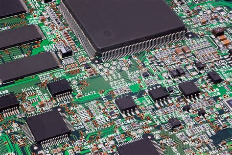
PCB stands for printed circuit board. It is the foundation of nearly all modern electronic devices. PCBs are flat boards made of insulating materials like fiberglass, with conductive copper traces printed on them in a specific pattern. Electronic components like microchips, resistors, and capacitors are then soldered onto the board to form a functional circuit.
PCB technology enables the miniaturization and mass production of complex electronics. Some key advantages of PCBs include:
- Compact size and light weight
- Low manufacturing cost at high volumes
- Reliability and durability
- Design flexibility and repeatability
PCBs are found in everything from smartphones and laptops to medical devices, automobiles, aerospace equipment, and industrial machinery. The global PCB market size was valued at over $60 billion in 2020 and is projected to continue steady growth in the coming years.
Skills of a PCB Engineer
A PCB engineer is responsible for designing and developing printed circuit boards. This requires a blend of electrical engineering knowledge and practical skills in CAD software, manufacturing processes, and testing/debugging. Some of the core competencies for a PCB engineer include:
1. Circuit Design
A strong foundation in electrical engineering principles is essential. PCB engineers must be able to design circuits that meet the functional requirements and design constraints of the end application. This involves selecting appropriate components, creating schematics, performing simulations, and validating the design.
2. PCB Layout
Once the schematic is finalized, it must be translated into a physical PCB layout using computer-aided design (CAD) software. The PCB layout defines the location and routing of all the components and copper traces on the board. Proper PCB layout is critical to ensure signal integrity, power delivery, thermal management, and manufacturability.
Some key considerations in PCB layout include:
- Component placement
- Trace routing and spacing
- Power and ground planes
- Electromagnetic compatibility (EMC)
- Design for manufacturing (DFM) rules
Popular PCB layout software tools include Altium Designer, Cadence Allegro, Mentor Graphics PADS, and KiCad.
3. Manufacturing Process Knowledge
PCB engineers need to understand the various manufacturing processes used to fabricate PCBs and how design choices impact manufacturability and cost. The main steps in PCB manufacturing are:
- Printing circuit pattern on copper-clad laminate
- Etching away unwanted copper
- Drilling holes for vias and component leads
- Plating copper in holes to form conductive links
- Applying solder mask and silkscreen
- Surface finish (e.g. HASL, ENIG)
- Electrical testing
Different applications may require specialized manufacturing capabilities such as:
| Process | Description | Applications |
|---|---|---|
| HDI | High density interconnect with micro-vias and fine pitch | Smartphones, wearables |
| Flex / Rigid-Flex | Use flexible or combination of rigid and flex substrates | Fold able devices, automotive |
| Metal Core | Metal base for enhanced thermal dissipation | High-power LEDs, automotive lighting |
4. Assembly and Testing
PCB engineers work closely with the assembly team to ensure the PCB can be manufactured reliably and cost-effectively. They may need to specify the bill of materials (BOM), assembly drawings, and work instructions.
Designing for assembly (DFA) involves considerations such as:
- Component selection (size, pitch, packaging)
- Panelization and tooling holes
- Solder paste stencil design
- Fiducial marks for machine vision alignment
PCB engineers are also responsible for developing and executing test plans to verify the functionality, reliability, and compliance of the manufactured PCBs. This may include:
- In-circuit testing (ICT)
- Flying probe testing
- Boundary scan testing (JTAG)
- Functional testing
- Environmental stress testing
5. Documentation and Communication
Thorough documentation is important throughout the PCB design and development process. PCB engineers generate various deliverables such as:
- Design specifications
- Schematics
- Layout files
- Gerber files
- Bill of Materials (BOM)
- Assembly drawings
- Test plans and reports
Effective communication skills are also valuable to collaborate with cross-functional teams including electrical, mechanical, software, quality, and supply chain. PCB engineers often participate in design reviews to present and defend their design choices.

Career Prospects for PCB Engineers
PCB engineering offers good career prospects due to the ever-growing demand for electronics across industries. According to the U.S. Bureau of Labor Statistics, the median annual wage for electronics engineers was $107,540 in May 2020, and employment is projected to grow 3 percent from 2019 to 2029.
Entry-level PCB engineer roles typically require a bachelor’s degree in electrical engineering or related field. Some employers may prefer candidates with relevant experience through internships or projects.
With experience, PCB engineers can advance to senior, lead, or manager roles. Some may specialize in specific areas like signal integrity, EMC, or DFM. Others may transition to related roles such as application engineer, sales engineer, or technical marketing.
Continuing education and professional development are important to keep up with evolving technologies and industry best practices. Resources for PCB engineers include:
- Conferences (PCB West, PCB2Day, AltiumLive)
- Online courses (LinkedIn Learning, Udemy)
- Certifications (CID, CID+)
- Professional organizations (IPC, SMTA, IEEE)

Future Trends in PCB Technology
PCB technology continues to advance to enable smaller, faster, and more integrated electronic products. Some key trends shaping the future of PCBs include:
Advanced Packaging
Traditional surface mount (SMT) packaging is reaching its limits in terms of size and density. Advanced packaging technologies are emerging to enable 3D stacking of dies and embedding of components within the PCB substrate. Examples include:
- System-in-Package (SiP)
- Fan-out wafer-level packaging (FOWLP)
- Embedded die packaging
Substrate Materials
New substrate materials are being developed to improve the performance and functionality of PCBs. Some examples are:
- High-frequency laminates for 5G communications
- Metal core substrates for high-power LEDs
- Flexible and stretchable substrates for wearables
Printed Electronics
Advances in conductive inks and printing processes are enabling PCB to be produced by additive manufacturing methods like inkjet and screen printing. This allows for more design freedom, faster prototyping, and lower cost for low-volume production.
Printed electronics also enable new form factors such as:
– In-mold electronics (IME)
– Stretchable circuits
– 3D structural electronics
AI-Assisted Design
Artificial intelligence (AI) and machine learning (ML) are being applied to automate and optimize various aspects of PCB design, such as:
- Component selection and placement
- Routing and Layout
- Design rule checking (DRC)
- Simulation and verification
AI-assisted design tools can help improve design efficiency, reduce errors, and explore a larger solution space to find the optimal design.

Frequently Asked Questions (FAQ)
1. What education is required to become a PCB engineer?
Most PCB engineer roles require a bachelor’s degree in electrical engineering or related field. Some positions may accept an associate’s degree or relevant work experience. Continuing education and professional development are also important to keep up with new technologies and best practices.
2. What software tools do PCB engineers use?
PCB engineers use various computer-aided design (CAD) software for schematic capture, PCB layout, and simulation. Popular tools include Altium Designer, Cadence Allegro, Mentor Graphics PADS, Eagle, KiCad, and DesignSpark PCB. They may also use general-purpose tools like MATLAB and Python for analysis and automation.
3. What are some common challenges in PCB design?
Some common challenges include managing signal integrity, power integrity, and electromagnetic compatibility (EMC) as designs become more complex and high-speed. Ensuring manufacturability and reliability while minimizing cost is also a constant challenge. Keeping up with new technologies, standards, and supply chain constraints also requires continuous learning and adaptation.
4. What is the job outlook for PCB engineers?
The demand for PCB engineers is generally strong and stable, driven by the increasing electronics content across industries. The U.S. Bureau of Labor Statistics projects a 3% growth in employment of electronics engineers from 2019 to 2029. However, the job market can be affected by economic cycles and shifts in the electronics industry.
5. How can I advance my career as a PCB engineer?
PCB engineers can advance their careers by taking on more complex and high-profile projects, mentoring junior engineers, and continuously updating their skills. Some may choose to specialize in areas like signal integrity, DFM, or embedded systems. Others may move into leadership roles like technical lead, engineering manager, or director. Networking, publishing, and presenting at conferences can also help raise one’s profile in the industry.


Leave a Reply