Introduction to PCB Fabrication
Printed Circuit Board (PCB) fabrication is a multi-step process that involves creating a functional circuit board from a design layout. The PCB fabrication process has evolved over the years with advancements in technology, materials, and manufacturing techniques. In this article, we will explore the various steps involved in PCB fabrication and the different PCB manufacturing techniques used in the industry.
What is PCB Fabrication?
PCB fabrication is the process of creating a functional printed circuit board from a design layout. The process involves several steps, including design, printing, etching, drilling, plating, solder mask application, silkscreen printing, and testing. The end result is a functional PCB that can be used in various electronic devices and applications.
Key Steps in the PCB Fabrication Process
-
Design: The first step in PCB fabrication is designing the circuit board layout using CAD software. The design includes the placement of components, traces, vias, and other features.
-
Printing: Once the design is finalized, it is printed onto a copper-clad laminate board using a photoresist process. The photoresist is a light-sensitive material that hardens when exposed to light.
-
Etching: After printing, the board is exposed to a chemical solution that etches away the unwanted copper, leaving only the desired traces and pads.
-
Drilling: Holes are drilled into the board to allow for the placement of components and vias.
-
Plating: The holes and traces are plated with a thin layer of copper to improve conductivity and durability.
-
Solder Mask Application: A solder mask is applied to the board to protect the copper traces from oxidation and prevent short circuits.
-
Silkscreen Printing: Text and symbols are printed onto the board using silkscreen printing to aid in assembly and identification.
-
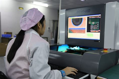
Testing: The completed board is tested for functionality and quality before being shipped to the customer.

PCB Manufacturing Techniques
There are several PCB manufacturing techniques used in the industry, each with its own advantages and disadvantages. The choice of manufacturing technique depends on factors such as the complexity of the design, the required volume, and the budget.
Through-Hole Technology
Through-hole technology is one of the oldest PCB manufacturing techniques. It involves drilling holes into the board and inserting components with leads that are soldered onto the other side of the board. Through-hole technology is reliable and durable but is limited in terms of component density and requires more manual labor.
Surface Mount Technology (SMT)
Surface mount technology is a more modern PCB manufacturing technique that involves placing components directly onto the surface of the board. SMT allows for higher component density and faster assembly times compared to through-hole technology. However, it requires specialized equipment and skilled operators.
Mixed Technology
Mixed technology combines both through-hole and surface mount components on the same board. This technique is useful for designs that require both types of components or for transitioning from through-hole to surface mount technology.
High Density Interconnect (HDI)
High density interconnect is a PCB manufacturing technique that involves creating multiple layers of interconnects within the board. HDI allows for higher component density and smaller form factors compared to traditional PCB manufacturing techniques. However, it is more expensive and requires specialized equipment and expertise.

Advantages of PCB Fabrication
PCB fabrication offers several advantages over traditional point-to-point wiring and breadboarding techniques. Some of the key advantages include:
-
Reliability: PCBs are more reliable than point-to-point wiring due to their fixed layout and improved insulation.
-
Efficiency: PCBs can be mass-produced using automated manufacturing techniques, reducing the time and cost of production.
-
Miniaturization: PCBs allow for smaller form factors and higher component density compared to traditional wiring techniques.
-
Standardization: PCBs can be designed to meet industry standards and specifications, ensuring compatibility with other electronic components and devices.

Challenges in PCB Fabrication
Despite the many advantages of PCB fabrication, there are also several challenges that manufacturers face. Some of the key challenges include:
-
Complexity: As electronic devices become more complex, PCB designs are also becoming more intricate and challenging to manufacture.
-
Material Costs: The cost of raw materials used in PCB fabrication, such as copper and laminate, can fluctuate based on market conditions and supply chain disruptions.
-
Regulatory Compliance: PCB manufacturers must comply with various regulatory standards and requirements related to environmental impact, safety, and quality control.
-
Skilled Labor: PCB fabrication requires skilled operators and technicians who are knowledgeable in the various manufacturing techniques and processes.
Future Trends in PCB Fabrication
As technology continues to evolve, so too will the PCB fabrication industry. Some of the future trends in PCB fabrication include:
-
3D Printing: 3D printing technology is being explored as a potential solution for rapid prototyping and small-scale production of PCBs.
-
Flexible and Stretchable PCBs: Flexible and stretchable PCBs are being developed for use in wearable devices, medical applications, and other areas where traditional rigid PCBs are not suitable.
-
Embedded Components: PCB manufacturers are exploring ways to embed components directly into the board, reducing the need for additional assembly steps and improving reliability.
-
Sustainable Materials: There is a growing demand for sustainable and eco-friendly materials in PCB fabrication, such as biodegradable and recyclable laminates.
PCB Fabrication Process Flow
The PCB fabrication process flow typically involves the following steps:
| Step | Description |
|---|---|
| 1 | Design |
| 2 | Printing |
| 3 | Etching |
| 4 | Drilling |
| 5 | Plating |
| 6 | Solder Mask Application |
| 7 | Silkscreen Printing |
| 8 | Testing |
Frequently Asked Questions (FAQ)
1. What is the difference between through-hole and surface mount technology?
Through-hole technology involves drilling holes into the board and inserting components with leads that are soldered onto the other side of the board. Surface mount technology involves placing components directly onto the surface of the board without the need for holes.
2. What is the purpose of solder mask in PCB fabrication?
Solder mask is a protective layer applied to the copper traces on a PCB to prevent oxidation and short circuits. It also helps to prevent solder from bridging between adjacent pads during the assembly process.
3. What is the advantage of using high density interconnect (HDI) in PCB fabrication?
High density interconnect allows for higher component density and smaller form factors compared to traditional PCB manufacturing techniques. This is achieved by creating multiple layers of interconnects within the board.
4. What are some of the challenges faced by PCB manufacturers?
Some of the challenges faced by PCB manufacturers include increasing complexity of designs, fluctuating material costs, regulatory compliance, and the need for skilled labor.
5. What are some future trends in PCB fabrication?
Some future trends in PCB fabrication include 3D printing, flexible and stretchable PCBs, embedded components, and the use of sustainable materials.
Conclusion
PCB fabrication is a critical process in the electronics industry, enabling the creation of functional circuit boards for a wide range of applications. The process involves several steps, from design to testing, and requires specialized equipment and expertise. PCB manufacturers face several challenges, including increasing complexity of designs, material costs, and regulatory compliance. However, the industry is also exploring new technologies and trends, such as 3D printing, flexible and stretchable PCBs, and sustainable materials. As technology continues to evolve, the PCB fabrication industry will need to adapt and innovate to meet the changing needs of the market.


Leave a Reply