Introduction to Peelable Solder Mask
Peelable solder mask, also known as temporary solder mask or peelable mask, is a special type of solder mask used in printed circuit board (PCB) manufacturing. Unlike regular permanent solder masks that remain on the PCB throughout its lifecycle, peelable solder mask is designed to be removed after specific soldering processes are complete. This unique property makes peelable solder mask an essential tool for various applications in PCB fabrication and assembly.
In this comprehensive article, we will dive deep into the world of peelable solder mask, exploring its composition, applications, advantages, and the process of using it in PCB manufacturing. We will also address some frequently asked questions to help you better understand this innovative material.
What is Solder Mask?
Before we delve into the specifics of peelable solder mask, let’s first understand what solder mask is and its role in PCB manufacturing.
Solder mask, also called solder resist or solder stop, is a thin layer of polymer applied to the copper traces of a PCB. Its primary purpose is to protect the copper from oxidation and prevent solder bridges from forming between closely spaced pads during the soldering process. Solder mask also provides electrical insulation, improves the PCB’s appearance, and helps users identify different components and features on the board.
Solder mask is typically applied using screen printing or photoimaging techniques, and it comes in various colors, with green being the most common. The choice of color can be based on aesthetic preferences, industry standards, or functional requirements, such as enhancing contrast for better visual inspection.

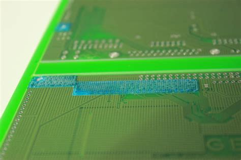
Composition and Properties of Peelable Solder Mask
Peelable solder mask is a specially formulated polymer designed to provide temporary protection during specific soldering processes. It is typically composed of a base resin, solvents, fillers, and additives that impart its unique properties.
The base resin in peelable solder mask is usually an acrylic or vinyl-based polymer that provides the necessary film-forming properties and adhesion to the PCB surface. Solvents help in maintaining the proper viscosity of the mixture for easy application and drying. Fillers, such as silica or alumina, improve the mechanical strength and thermal stability of the mask. Finally, additives, such as plasticizers, defoamers, and wetting agents, enhance the overall performance and ease of use.
One of the key properties of peelable solder mask is its ability to withstand high temperatures during soldering processes. It typically has a temperature resistance of up to 150°C, allowing it to protect the PCB surface during wave soldering or Selective Soldering operations.
Another crucial property is its ease of removal after the soldering process is complete. Peelable solder mask is designed to form a strong, yet flexible film that can be easily peeled off without leaving residues or damaging the underlying PCB surface. This property is achieved through careful formulation and optimization of the resin, fillers, and additives.

Advantages of Using Peelable Solder Mask
Peelable solder mask offers several advantages over traditional permanent solder masks in specific PCB manufacturing scenarios:
-
Selective Soldering: Peelable solder mask allows for selective soldering of components on a PCB. By masking off areas that need to be soldered later or require different soldering processes, manufacturers can improve efficiency and reduce the risk of damage to sensitive components.
-
Rework and Repair: In case of soldering defects or component failures, peelable solder mask simplifies the rework and repair process. The mask can be easily removed to access the affected area, and a new layer can be applied after the repair is complete.
-
Prototyping and Testing: Peelable solder mask is ideal for prototyping and testing PCBs, as it allows for quick modifications and iterations. Engineers can apply and remove the mask as needed to test different configurations or make design changes.
-
Improved Aesthetics: Peelable solder mask can be used to create temporary markings, logos, or text on the PCB surface. This can be useful for branding, labeling, or providing instructions during the manufacturing process.
-
Cost Savings: In some cases, using peelable solder mask can help reduce overall manufacturing costs. By eliminating the need for multiple permanent solder mask applications or reducing the number of processing steps, manufacturers can optimize their production workflow and minimize material waste.

Applications of Peelable Solder Mask
Peelable solder mask finds applications in various aspects of PCB manufacturing and assembly:
-
Wave Soldering: Peelable solder mask is commonly used in wave soldering processes to protect specific areas of the PCB from solder exposure. By masking off regions that don’t require soldering, manufacturers can prevent bridges, shorts, or unintended connections.
-
Selective Soldering: In selective soldering, peelable solder mask allows for targeted soldering of specific components or areas on the PCB. This is particularly useful when dealing with high-density boards or components with varying soldering requirements.
-
Conformal Coating: Peelable solder mask can be used as a temporary mask for applying conformal coating to PCBs. By masking off areas that don’t require coating, manufacturers can ensure precise and uniform coverage.
-
Solder Paste Application: In some cases, peelable solder mask can be used to create temporary stencils for applying solder paste to PCB pads. This can be an alternative to metal stencils, particularly for low-volume or prototype production runs.
-
Electrical Testing: Peelable solder mask can be used to isolate specific areas of the PCB during electrical testing. By masking off certain regions, engineers can perform targeted tests and measurements without interference from other components.
Process of Using Peelable Solder Mask
The process of using peelable solder mask in PCB manufacturing involves several steps:
-
Surface Preparation: Before applying the peelable solder mask, the PCB surface must be clean, dry, and free from contaminants. This ensures proper adhesion and uniform coverage of the mask.
-
Application: Peelable solder mask can be applied using various methods, such as screen printing, spraying, or dipping. The choice of application method depends on the specific requirements of the PCB, the desired thickness of the mask, and the available equipment.
-
Drying and Curing: After application, the peelable solder mask must be dried and cured to form a stable film. This typically involves exposing the PCB to heat or UV light, depending on the specific formulation of the mask. Proper drying and curing ensure that the mask achieves its desired properties and can withstand the subsequent soldering processes.
-
Soldering: With the peelable solder mask in place, the PCB can undergo the required soldering processes, such as wave soldering or selective soldering. The mask protects the designated areas from solder exposure while allowing the desired connections to be formed.
-
Removal: Once the soldering process is complete, the peelable solder mask can be removed. This is typically done by gently peeling off the mask, starting from a corner or edge. The removal process should not leave any residues or damage the PCB surface.
-
Inspection and Cleaning: After removing the peelable solder mask, the PCB should be inspected for any defects or residues. If necessary, the board can be cleaned using appropriate solvents or cleaning agents to ensure a pristine surface for the next steps in the manufacturing process.
Peelable Solder Mask vs. Permanent Solder Mask
While peelable solder mask and permanent solder mask serve similar purposes in PCB manufacturing, they have distinct differences in their properties and applications. Here’s a comparison table highlighting the key aspects:
| Property | Peelable Solder Mask | Permanent Solder Mask |
|---|---|---|
| Composition | Acrylic or vinyl-based polymers, solvents, fillers, and additives | Epoxy, acrylic, or polyurethane-based polymers, fillers, and additives |
| Application | Screen printing, spraying, or dipping | Screen printing or photoimaging |
| Curing | Heat or UV light | UV light or thermal curing |
| Temperature Resistance | Up to 150°C | Up to 150°C or higher |
| Removal | Easily peelable | Permanent, not removable |
| Thickness | Typically thicker than permanent solder mask | Thinner, around 0.01-0.03mm |
| Durability | Temporary protection | Long-lasting protection |
| Applications | Selective soldering, rework, prototyping, conformal coating | Full PCB Protection, component identification, insulation |
As evident from the table, peelable solder mask and permanent solder mask differ in their composition, application methods, removal properties, and intended use cases. While peelable solder mask offers temporary protection and flexibility, permanent solder mask provides long-lasting coverage and serves additional functions like component identification and insulation.
Choosing the Right Peelable Solder Mask
When selecting a peelable solder mask for your PCB manufacturing process, consider the following factors:
-
Compatibility: Ensure that the peelable solder mask is compatible with your PCB substrate material, soldering processes, and any additional coatings or treatments used in your manufacturing workflow.
-
Temperature Resistance: Choose a peelable solder mask that can withstand the maximum temperature encountered during your soldering processes. Most peelable masks can resist temperatures up to 150°C, but some specialized formulations may offer higher temperature resistance.
-
Ease of Application: Consider the application method that best suits your manufacturing setup and PCB design. Some peelable solder masks are formulated for screen printing, while others may be optimized for spraying or dipping.
-
Removal Characteristics: Look for a peelable solder mask that can be easily and cleanly removed without leaving residues or damaging the PCB surface. The mask should have good adhesion during the soldering process but still allow for effortless peeling when required.
-
Drying and Curing Requirements: Select a peelable solder mask that is compatible with your existing drying and curing equipment. Some masks may require specific heat or UV light exposure settings to achieve optimal performance.
-
Environmental and Safety Considerations: Opt for peelable solder masks that comply with relevant environmental and safety regulations. Look for products with low volatile organic compound (VOC) content and those that are RoHS (Restriction of Hazardous Substances) compliant.
-
Cost-Effectiveness: Evaluate the cost of the peelable solder mask in relation to its performance and the specific requirements of your PCB manufacturing process. Consider factors such as material consumption, process efficiency improvements, and potential cost savings in terms of reduced rework or simplified workflows.
Frequently Asked Questions (FAQ)
-
Q: Can peelable solder mask be used on any type of PCB substrate?
A: Peelable solder mask is generally compatible with most common PCB substrate materials, such as FR-4, polyimide, and aluminum. However, it’s essential to verify compatibility with your specific substrate and any additional surface treatments or coatings used in your manufacturing process. -
Q: How thick is a typical layer of peelable solder mask?
A: The thickness of a peelable solder mask layer can vary depending on the application method and the specific product used. Generally, peelable masks are thicker than permanent solder masks, with typical thicknesses ranging from 0.05mm to 0.2mm. -
Q: Can peelable solder mask be reapplied after removal?
A: In most cases, peelable solder mask can be reapplied after removal, as long as the PCB surface is clean and free from residues. However, it’s important to follow the manufacturer’s guidelines for reapplication to ensure optimal performance and adhesion. -
Q: How do I store and handle peelable solder mask?
A: Peelable solder mask should be stored in a cool, dry place, away from direct sunlight and sources of heat or moisture. Follow the manufacturer’s recommendations for storage temperature and shelf life. When handling the mask, use appropriate personal protective equipment (PPE) such as gloves and safety glasses, and work in a well-ventilated area. -
Q: Are there any limitations or challenges associated with using peelable solder mask?
A: While peelable solder mask offers several advantages, there are a few limitations to consider. Peelable masks may not provide the same level of durability and long-term protection as permanent solder masks. They may also require additional processing steps and handling compared to traditional solder masks. Additionally, some peelable masks may have limitations in terms of minimum feature size or resolution, depending on the application method used.
Conclusion
Peelable solder mask is a versatile and innovative material that offers unique advantages in PCB manufacturing. Its ability to provide temporary protection, enable selective soldering, and simplify rework and repair processes makes it an essential tool for many applications.
By understanding the composition, properties, and applications of peelable solder mask, PCB Manufacturers can leverage its benefits to optimize their production workflows, improve quality, and reduce costs. However, it’s crucial to carefully select the right peelable solder mask product based on compatibility, performance, and process requirements.
As PCB designs continue to evolve and become more complex, the use of peelable solder mask is likely to grow in importance. Manufacturers that adopt this technology and integrate it effectively into their processes will be well-positioned to meet the ever-increasing demands of the electronics industry.
In conclusion, peelable solder mask is a valuable addition to the PCB Manufacturer’s toolkit, offering flexibility, efficiency, and innovation in an increasingly competitive and dynamic market.


Leave a Reply