Understanding PCB Protection
What are PCBs?
PCBs, or Printed Circuit Boards, are the backbone of modern electronic devices. They are the green boards that hold all the electronic components together and allow them to communicate with each other. PCBs are found in almost every electronic device, from smartphones and laptops to medical equipment and aerospace systems.
Why is PCB Protection Important?
PCB protection is crucial for several reasons:
- Reliability: Protecting PCBs from damage ensures that the electronic device functions reliably and consistently over its intended lifespan.
- Safety: Proper PCB protection minimizes the risk of electrical hazards, such as short circuits or fires, which can be dangerous to users and the environment.
- Cost-effectiveness: Implementing PCB protection measures during the design and manufacturing stages can prevent costly repairs or replacements down the line.
Common Threats to PCBs
PCBs are exposed to various threats that can compromise their integrity and functionality. Some of these threats include:
- Environmental factors: Moisture, dust, and extreme temperatures can damage PCBs over time.
- Mechanical stress: Vibrations, shocks, and impacts can cause physical damage to PCBs and their components.
- Electromagnetic Interference (EMI): External electromagnetic fields can interfere with the operation of PCBs and cause signal integrity issues.
- Electrostatic Discharge (ESD): Sudden discharges of static electricity can damage sensitive electronic components on the PCB.
PCB Protection Techniques
Conformal Coating
Conformal coating is a popular method for protecting PCBs from environmental factors, such as moisture and dust. It involves applying a thin layer of protective material, such as acrylic, silicone, or polyurethane, over the surface of the PCB and its components.
Advantages of conformal coating:
– Provides a barrier against moisture, dust, and other contaminants
– Helps to insulate the PCB and prevent short circuits
– Can be easily applied using various methods, such as spraying, dipping, or brushing
Disadvantages of conformal coating:
– Can be difficult to remove for repairs or modifications
– May not be suitable for all components, such as connectors or switches
– Requires proper surface preparation and curing for optimal performance
| Conformal Coating Material | Advantages | Disadvantages |
|---|---|---|
| Acrylic | Easy to apply and remove, good moisture resistance | Limited temperature range, less durable than other options |
| Silicone | Excellent temperature and humidity resistance, good flexibility | More expensive, can be difficult to apply evenly |
| Polyurethane | High abrasion and chemical resistance, good dielectric properties | Requires more curing time, can be difficult to remove |
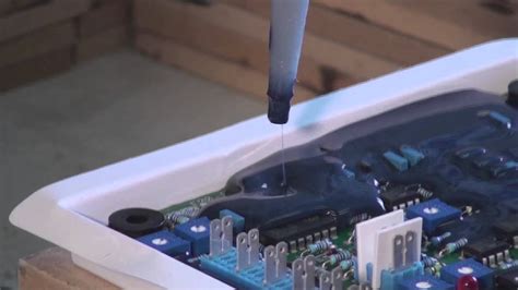
Potting
Potting involves encapsulating the PCB and its components in a solid compound, such as epoxy or silicone. This method provides excellent protection against mechanical stress, moisture, and other environmental factors.
Advantages of potting:
– Offers superior protection against vibrations, shocks, and impacts
– Creates a strong barrier against moisture and other contaminants
– Can help to dissipate heat from the PCB and its components
Disadvantages of potting:
– Permanent encapsulation makes repairs or modifications difficult
– Adds significant weight and bulk to the PCB Assembly
– Requires careful design considerations for proper compound selection and application
Shielding
Shielding is a technique used to protect PCBs from electromagnetic interference (EMI). It involves enclosing the PCB or specific components in a conductive material, such as metal or conductive plastic, to create a Faraday cage that blocks external electromagnetic fields.
Advantages of shielding:
– Effectively reduces EMI and improves signal integrity
– Can be customized to target specific frequency ranges or components
– Helps to comply with EMC (Electromagnetic Compatibility) regulations
Disadvantages of shielding:
– Adds cost and complexity to the PCB design and assembly process
– May require additional grounding and bonding measures for optimal performance
– Can limit access to components for debugging or repairs
ESD Protection
Electrostatic Discharge (ESD) protection is essential for safeguarding sensitive electronic components on the PCB from sudden discharges of static electricity. ESD protection can be implemented through various methods, such as:
- ESD-safe handling procedures: Implementing proper handling procedures, such as using grounded wrist straps and ESD-safe workstations, can minimize the risk of ESD damage during PCB assembly and handling.
- ESD protection components: Installing ESD protection components, such as transient voltage suppressors (TVS) or multilayer Varistors (MLV), can help to divert and dissipate ESD energy before it reaches sensitive components.
- PCB layout techniques: Proper PCB layout techniques, such as minimizing trace lengths, using guard rings, and providing adequate grounding, can help to reduce the impact of ESD events on the PCB.
| ESD Protection Method | Advantages | Disadvantages |
|---|---|---|
| ESD-safe handling procedures | Low cost, easy to implement | Relies on consistent adherence to procedures |
| ESD protection components | Provides targeted protection for sensitive components | Adds cost and complexity to the PCB design |
| PCB layout techniques | Can be implemented during the design phase, no additional components required | Requires careful planning and may compromise other design goals |

Best Practices for PCB Protection
Design for Manufacturability (DFM)
Designing PCBs with manufacturability in mind can help to ensure that the boards are robust and reliable. Some DFM considerations for PCB protection include:
- Selecting appropriate materials: Choose PCB materials that are suitable for the intended operating environment and can withstand the expected mechanical and thermal stresses.
- Providing adequate clearances: Ensure that there are sufficient clearances between components, traces, and board edges to minimize the risk of short circuits and physical damage.
- Optimizing component placement: Place components in a way that minimizes the impact of mechanical stress and allows for proper heat dissipation.
Testing and Validation
Thorough testing and validation are essential for ensuring that PCB protection measures are effective and meet the required performance standards. Some key testing and validation activities include:
- Environmental testing: Expose the PCB to various environmental conditions, such as temperature cycling, humidity, and vibration, to assess its durability and reliability.
- EMC testing: Test the PCB for electromagnetic compatibility to ensure that it does not emit excessive EMI and is not susceptible to external electromagnetic fields.
- Functional testing: Verify that the PCB performs as intended under different operating conditions and scenarios.
Maintenance and Repair
Proper maintenance and repair practices can help to extend the lifespan of PCBs and minimize the impact of any protection failures. Some best practices include:
- Regular inspections: Conduct periodic inspections of the PCB to identify any signs of damage, corrosion, or degradation.
- Cleaning and refurbishment: Clean the PCB regularly to remove any contaminants or debris that may compromise its protection. If necessary, refurbish the PCB by reapplying conformal coating or replacing damaged components.
- Proper handling and storage: Follow ESD-safe handling procedures and store PCBs in a controlled environment to minimize the risk of damage during transportation and storage.

Frequently Asked Questions (FAQ)
-
What is the most common method for protecting PCBs from environmental factors?
Conformal coating is the most common method for protecting PCBs from environmental factors, such as moisture and dust. It involves applying a thin layer of protective material over the surface of the PCB and its components. -
Can potting be removed for repairs or modifications?
Potting is a permanent encapsulation method, which makes repairs or modifications difficult. In most cases, potted PCBs cannot be easily disassembled without damaging the components or the board itself. -
How does shielding protect PCBs from electromagnetic interference (EMI)?
Shielding involves enclosing the PCB or specific components in a conductive material, such as metal or conductive plastic, to create a Faraday cage. This cage blocks external electromagnetic fields, reducing EMI and improving signal integrity. -
What are some ESD protection components that can be used on PCBs?
Transient voltage suppressors (TVS) and multilayer varistors (MLV) are common ESD protection components that can be installed on PCBs. These components help to divert and dissipate ESD energy before it reaches sensitive components. -
How often should PCBs be inspected for signs of damage or degradation?
The frequency of PCB Inspections depends on the specific application and operating environment. As a general rule, PCBs should be inspected at least once a year or more frequently if they are exposed to harsh conditions or critical applications.

Conclusion
PCB protection is a critical aspect of electronic device design and manufacturing. By understanding the common threats to PCBs and implementing appropriate protection techniques, designers and manufacturers can ensure that their products are reliable, safe, and cost-effective.
From conformal coating and potting to shielding and ESD protection, there are various methods available to safeguard PCBs from environmental factors, mechanical stress, electromagnetic interference, and electrostatic discharge. By following best practices for design, testing, and maintenance, companies can optimize the performance and longevity of their PCBs and the electronic devices they power.
As technology continues to advance and the demand for more complex and reliable electronic systems grows, the importance of PCB protection will only continue to increase. By staying informed about the latest protection techniques and best practices, designers and manufacturers can stay ahead of the curve and deliver high-quality, robust PCBs that meet the evolving needs of their customers.


Leave a Reply