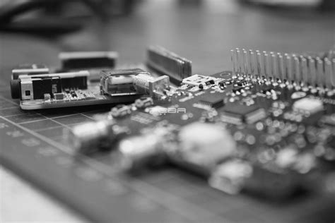
What is PCB Fabrication?
PCB fabrication is the process of designing and manufacturing printed circuit boards (PCBs). PCBs are essential components in electronic devices, serving as the foundation for connecting and supporting various electronic components. The fabrication process involves several steps, including design, material selection, etching, drilling, and finishing.
Steps in PCB Fabrication
- Design
- Material Selection
- Etching
- Drilling
- Finishing
| Step | Description |
|---|---|
| Design | Creating the PCB Layout using specialized software |
| Material Selection | Choosing the appropriate substrate material, such as FR-4 |
| Etching | Removing unwanted copper from the PCB surface |
| Drilling | Creating holes for component placement and vias |
| Finishing | Applying solder mask, silkscreen, and surface finish |
Circuit Board Repair Kit Tape and Pad
When it comes to PCB fabrication, circuit board repair kit tape and pad play a crucial role in ensuring the integrity and functionality of the finished product. These materials are used to protect sensitive components, provide insulation, and aid in the assembly process.
Types of Circuit Board Repair Kit Tape
- Polyimide Tape
- Kapton Tape
- Teflon Tape
- Copper Foil Tape
| Tape Type | Characteristics |
|---|---|
| Polyimide Tape | High-temperature resistance, excellent insulation properties |
| Kapton Tape | Thin, lightweight, and resistant to chemicals and solvents |
| Teflon Tape | Non-stick surface, high-temperature resistance |
| Copper Foil Tape | Conductive, used for shielding and grounding |
Applications of Circuit Board Repair Kit Tape
- Masking during soldering
- Insulating sensitive components
- Securing wires and cables
- Providing mechanical support

Pad PCB Fabrication
Pad PCB fabrication refers to the process of creating and placing pads on the PCB surface. Pads are small, flat, conductive areas that provide a connection point for electronic components. They are typically made of copper and can be plated with various finishes to improve solderability and durability.
Types of Pads in PCB Fabrication
- Surface Mount Pads (SMD)
- Through-Hole Pads (THT)
- Vias
- Testpoints
| Pad Type | Description |
|---|---|
| SMD Pads | Used for surface-mounted components |
| THT Pads | Used for through-hole components |
| Vias | Conductive holes that connect different layers of the PCB |
| Testpoints | Pads used for testing and debugging purposes |
Pad Design Considerations
- Size and shape
- Spacing and clearance
- Solder mask and paste
- Thermal management

Benefits of Using Circuit Board Repair Kit Tape and Pad in PCB Fabrication
- Improved reliability and durability
- Enhanced electrical performance
- Simplified assembly process
- Reduced manufacturing costs

Challenges in PCB Fabrication
Despite the advancements in technology and materials, PCB fabrication still faces several challenges. Some of these challenges include:
- Miniaturization
- High-speed design
- Material selection
- Environmental concerns
Miniaturization
As electronic devices become smaller and more compact, PCB fabrication must adapt to accommodate these changes. Miniaturization poses challenges in terms of component placement, routing, and thermal management.
High-Speed Design
With the increasing demand for high-speed electronic devices, PCB fabrication must address issues related to signal integrity, crosstalk, and electromagnetic interference (EMI). Proper design techniques and material selection are crucial in mitigating these challenges.
Material Selection
Choosing the right materials for PCB fabrication is essential for ensuring the performance and reliability of the finished product. Factors such as dielectric constant, thermal conductivity, and mechanical strength must be considered when selecting materials.
Environmental Concerns
PCB fabrication processes often involve the use of chemicals and materials that can have a negative impact on the environment. Manufacturers must adhere to strict regulations and implement eco-friendly practices to minimize their environmental footprint.
Future Trends in PCB Fabrication
As technology continues to evolve, PCB fabrication must keep pace with the latest trends and advancements. Some of the future trends in PCB fabrication include:
- 3D Printing
- Embedded Components
- Flexible and Stretchable PCBs
- Increased Automation
3D Printing
3D printing technology has the potential to revolutionize PCB fabrication by enabling the creation of complex, three-dimensional structures. This technology can be used to fabricate PCBs with embedded components, reducing the need for traditional assembly processes.
Embedded Components
Embedding components within the PCB substrate can help reduce the overall size of the board and improve its performance. This technique involves placing components inside the PCB Layers during the fabrication process, resulting in a more compact and efficient design.
Flexible and Stretchable PCBs
Flexible and stretchable PCBs are becoming increasingly popular in applications such as wearable electronics and medical devices. These PCBs can conform to complex shapes and withstand repeated bending and stretching without compromising their electrical performance.
Increased Automation
Automation is playing an increasingly important role in PCB fabrication, helping to improve efficiency, reduce costs, and minimize human error. Automated processes such as pick-and-place machines, optical inspection systems, and robotic assembly lines are becoming more common in PCB manufacturing facilities.
Frequently Asked Questions (FAQ)
- What is the difference between surface mount and through-hole components?
-
Surface mount components are mounted directly onto the surface of the PCB, while through-hole components have leads that are inserted into holes drilled in the board and soldered on the opposite side.
-
What is the purpose of solder mask in PCB fabrication?
-
Solder mask is a protective coating applied to the PCB surface that prevents solder from adhering to unwanted areas during the assembly process. It also provides insulation and protection against environmental factors.
-
What is the difference between single-sided and Double-sided PCBs?
-
Single-Sided PCBs have components and conductive traces on only one side of the board, while double-sided PCBs have components and traces on both sides, allowing for more complex designs and higher component density.
-
What is the role of vias in PCB fabrication?
-
Vias are conductive holes that connect different layers of a multi-layer PCB. They allow signals and power to be routed between layers, enabling more complex and compact designs.
-
What are the environmental considerations in PCB fabrication?
- PCB fabrication processes can involve the use of hazardous chemicals and materials, such as lead and halogenated flame retardants. Manufacturers must adhere to environmental regulations and implement eco-friendly practices, such as using lead-free solder and properly disposing of waste materials.
Conclusion
PCB fabrication is a complex and continuously evolving process that plays a crucial role in the development of modern electronic devices. Circuit board repair kit tape and pad are essential components in ensuring the performance and reliability of PCBs. As technology advances, PCB fabrication must adapt to new challenges and trends, such as miniaturization, high-speed design, and environmental concerns. By understanding the fundamentals of PCB fabrication and staying up-to-date with the latest advancements, manufacturers can create high-quality, reliable, and innovative electronic products.


Leave a Reply