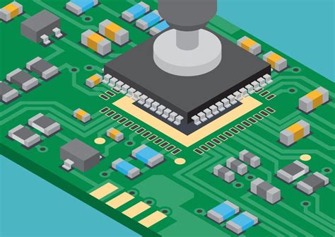
What is Surface-mount technology (SMT)?
Surface-mount technology is a method of assembling electronic components directly onto the surface of a printed circuit board. Unlike through-hole technology (THT), where component leads are inserted into holes drilled in the PCB and soldered on the opposite side, SMT components are placed and soldered directly onto the surface of the board. This technology has allowed for the miniaturization of electronic devices and has significantly increased the efficiency of the manufacturing process.
Advantages of SMT over THT
- Smaller component size
- Increased component density on PCBs
- Faster assembly process
- Reduced manufacturing costs
- Improved reliability and performance
SMT Components
SMT components are designed specifically for surface mounting on PCBs. These components come in various package types, each with its own characteristics and advantages.
Common SMT Package Types
| Package Type | Description | Advantages |
|---|---|---|
| Chip | Small, rectangular components with no leads | High component density, low cost |
| SOT | Small-Outline Transistor, compact transistor package | Suitable for high-frequency applications |
| QFP | Quad Flat Package, square or rectangular with leads on all four sides | High lead count, good thermal and electrical performance |
| BGA | Ball Grid Array, grid of solder balls underneath the component | High density, excellent electrical and thermal performance |
SMT Component Packaging
SMT components are typically supplied in one of three packaging types:
- Tape and Reel: Components are placed in pockets on a continuous tape, which is wound onto a reel for automated assembly.
- Tube: Components are packaged in plastic tubes, which can be used for manual or semi-automated assembly.
- Tray: Components are placed in pockets on a flat tray, which is suitable for manual assembly or low-volume production.

SMT Assembly Process
The SMT assembly process consists of several key steps, each of which is crucial for ensuring the quality and reliability of the final product.
Step 1: Solder Paste Application
Solder paste, a mixture of tiny solder particles and flux, is applied to the PCB using a stencil printing process. The stencil, a thin metal sheet with apertures corresponding to the component pads on the PCB, is aligned with the board. Solder paste is then spread across the stencil, filling the apertures and depositing the paste onto the pads.
Step 2: Component Placement
Once the solder paste is applied, the PCB moves to the pick-and-place machine. This automated system uses computer-controlled nozzles to pick up SMT components from feeders and place them precisely onto the solder paste-coated pads on the PCB. Modern pick-and-place machines can place thousands of components per hour with exceptional accuracy.
Step 3: Reflow Soldering
After component placement, the PCB enters the reflow soldering phase. The board is passed through a reflow oven, which heats the PCB and components according to a predetermined temperature profile. As the temperature increases, the solder paste melts, forming a strong mechanical and electrical connection between the components and the PCB pads. The temperature profile is carefully controlled to ensure proper solder joint formation and to prevent damage to the components.
Step 4: Inspection and Testing
Following the reflow soldering process, the assembled PCBs undergo inspection and testing to ensure the quality and functionality of the final product. Several methods are used, including:
- Visual Inspection: Manual or automated optical inspection to check for visible defects, such as misaligned components, solder bridges, or insufficient solder joints.
- Automated Optical Inspection (AOI): High-speed, high-resolution cameras compare the assembled PCB to a reference image, detecting any anomalies or defects.
- X-Ray Inspection: Used for examining solder joints hidden under components, such as BGA packages, to ensure proper solder joint formation.
- In-Circuit Testing (ICT): Electrical testing of individual components and circuits on the PCB to verify their functionality and compliance with specifications.
- Functional Testing: Testing the assembled PCB as a complete system to ensure it performs as intended in the final application.

SMT Process Challenges and Solutions
While SMT offers numerous advantages, there are also several challenges associated with the process. Manufacturers must address these challenges to ensure the production of high-quality, reliable electronic products.
Challenge 1: Miniaturization
As electronic devices continue to shrink in size, SMT components are also becoming smaller. This miniaturization poses challenges in terms of component handling, placement accuracy, and solder joint reliability.
Solutions:
– Invest in advanced pick-and-place machines with higher precision and smaller nozzle sizes.
– Implement more stringent process controls and monitoring to maintain placement accuracy.
– Use specialized solder paste formulations designed for miniaturized components.
Challenge 2: Thermal Management
With the increasing density of components on PCBs, thermal management becomes a critical issue. Proper heat dissipation is essential to prevent component failure and ensure long-term reliability.
Solutions:
– Incorporate thermal management techniques, such as the use of thermal vias, heat sinks, or thermal interface materials.
– Optimize PCB layout and component placement to minimize thermal hotspots and improve heat dissipation.
– Use thermally enhanced PCB substrates, such as Metal-Core PCBs or insulated metal substrates (IMS).
Challenge 3: Counterfeit Components
Counterfeit electronic components pose a significant risk to the electronics industry, leading to reduced reliability, performance issues, and potential safety hazards.
Solutions:
– Implement a robust supply chain management system to ensure the authenticity of components.
– Purchase components from authorized distributors or directly from manufacturers.
– Perform incoming inspection and testing to identify and prevent the use of counterfeit components.

Frequently Asked Questions (FAQ)
-
Q: What is the difference between SMT and through-hole technology?
A: SMT components are mounted directly onto the surface of the PCB, while through-hole components have leads that are inserted into holes drilled in the PCB and soldered on the opposite side. -
Q: Can SMT and through-hole components be used on the same PCB?
A: Yes, it is possible to use both SMT and through-hole components on the same PCB. This is known as a mixed-technology PCB Assembly. -
Q: What are the advantages of using SMT over through-hole technology?
A: SMT offers several advantages, including smaller component size, increased component density, faster assembly process, reduced manufacturing costs, and improved reliability and performance. -
Q: How does the reflow soldering process work in SMT assembly?
A: During reflow soldering, the PCB with solder paste and placed components is passed through a reflow oven. The oven heats the PCB according to a predetermined temperature profile, melting the solder paste and forming a strong mechanical and electrical connection between the components and the PCB pads. -
Q: What are some common challenges faced in the SMT process, and how can they be addressed?
A: Common challenges in the SMT process include miniaturization, thermal management, and counterfeit components. These challenges can be addressed by investing in advanced equipment, implementing strict process controls, optimizing PCB layouts, and ensuring a robust supply chain management system.
In conclusion, surface-mount technology has revolutionized the electronics manufacturing industry, enabling the production of smaller, more complex, and more reliable electronic devices. By understanding the SMT process, its advantages, and the various steps involved, manufacturers can optimize their assembly processes and overcome the challenges associated with this technology. As electronic devices continue to evolve, SMT will remain a critical aspect of the electronics industry, driving innovation and shaping the future of electronic products.


Leave a Reply