
Introduction to Rigid Flex PCBs
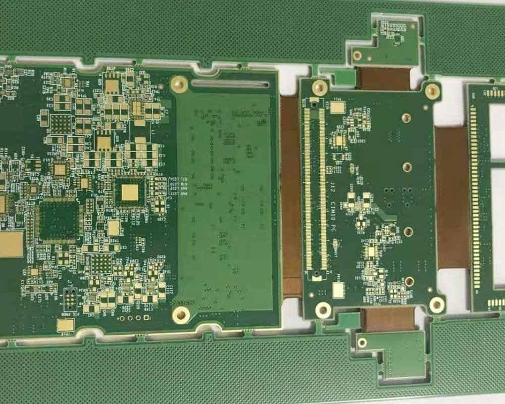
A rigid flex PCB (also known as flex-rigid PCB) combines rigid and flexible PCB technologies into one circuit board. Rigid flex PCBs contain both rigid sections – made of typical PCB substrates like FR-4 – and flexible sections made of polyimide or other flexible dielectric materials. The rigid sections provide mechanical support while the flexible sections allow dynamic flexing, bending or folding of the circuit board.
Rigid flex PCBs open up new possibilities in product design and miniaturization that are not possible with rigid PCBs alone. By embedding flexible sections into the PCB, rigid flex allows three-dimensional shaping and dense component mounting not achievable on a flat rigid board. This enables more compact product enclosures, complex form factors, and simplified mechanical designs. Rigid flex PCBs are commonly used for the following applications:
- Wearable devices
- Medical devices
- Military avionics
- Consumer electronics
- Automotive electronics
- Robotics
Below we dive into the key considerations and best practices for designing a reliable rigid flex PCB.
Rigid Flex PCB Materials
The material selection is critical in a rigid flex design. The rigid and flexible sections will use different base materials that must be compatible with each other.
Rigid Sections
The rigid portions of a rigid flex PCB typically use FR-4 or other common rigid PCB substrates. FR-4 with its woven glass reinforcement provides the needed structural support once the board is populated with components. Popular rigid substrate thicknesses range from 0.4mm to 2.0mm.
Flexible Sections
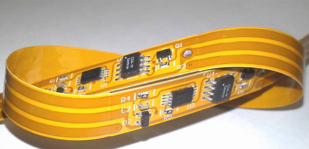
The flexible sections use a flexible dielectric material such as polyimide (Kapton). Other flexible materials include polyester (PET), PEN, polyethylene and PTFE. Polyimide is often preferred due to its excellent thermal stability and chemical resistance. Flexible sections are usually much thinner than rigid sections, with thicknesses ranging from 25μm to 150μm.
In single-layer flex constructions, a flexible adhesive layer is also required to bond the foil traces to the base polyimide. Common adhesive types are acrylic, epoxy and polyimide. The adhesive must be chemically compatible with the polyimide to avoid delamination issues.
The table below summarizes some key properties of typical rigid flex materials:
| Material | Dielectric Constant | Loss Tangent | Thermal Stability |
|---|---|---|---|
| FR-4 | 4.4 | 0.02 | 130°C |
| Polyimide | 3.4 | 0.002 | 300°C |
| Flex Adhesive | 2.9-4.1 | 0.01-0.04 | 150-200°C |
Coverlayers
In multilayer rigid flex boards, additional coverlayers may be laminated to the outer surfaces for protection, improved reliability, and to allow further circuit traces. Common coverlayer materials include solder mask, acrylic or polyimide.
Layer Stackup Design
The cross-sectional layer stackup defines the layer configuration in a rigid flex PCB. Here are some key stackup design considerations:
- Determine number of rigid layers and flex layers needed
- Define rigid and flex layer thicknesses
- Minimize number of lamination cycles
- Ensure compatible material transitions between rigid and flex
- Include coverlayers as needed for protection
For example, a simple rigid flex stackup may contain:
- 2-layer 0.8mm rigid FR-4 sections
- Single-layer 25μm flex polyimide sections
- Solder mask coverlayers
More complex designs can include 10 or more metal layers with multiple rigid and flexible segments in the same PCB outline.
Rigid-to-Flex Transitions
An important aspect of rigid flex PCB design is managing the transitions between the thick rigid sections and thin flexible sections. To avoid mechanical issues, the transitions must be well-designed.
Controlled Material Transition
There must be a controlled material transition between the rigid and flex layers. An abrupt transition from a thick 1.6mm rigid section to a 25μm polyimide layer will be prone to delamination and cracking.
To create a smooth transition, additional flexible layers are often laminated in the transition area. For example, a 25μm flex dielectric may be laminated over the rigid layers, followed by a 50μm polyimide transition layer, before the full flex thickness. Some rigid layers may also be dropped sequentially in the transition region.
Teardrop Shapes
The outer shape of the PCB at the rigid-flex junction should use a teardrop shape rather than a sharp corner. This minimizes stress concentrations in the transition area. Other techniques like buried vias or filled holes near the transition can also relieve stresses.
Flex Bend Radius
The flexible area exiting the rigid section should bend in a controlled radius, typically 3-4x the flex layer thickness. Avoid sharp folds and creases than can damage the thin flex layers.
Trace Routing
Traces on flexible layers require special care:
- Use 1oz copper foil for better flexibility
- Keep line spacing and widths larger than normal
- Avoid traces perpendicular to the bend axis
- Run critical signals on inner layers
- Enable tear-stop plating at flex exits
It is best practice to keep high-speed signals and sensitive traces on the interior rigid layers whenever possible. The flexible layers are more prone to noise and mishandling damage.
For outer flex layers, the traces should route parallel to the bend axis as much as allowable. Perpendicular traces will see higher stress and propagation issues when flexed. Wider trace spacing and widths relieve stress on the foil. Tear-stop plating reinforces the traces at flex exits.
Component Placement
Follow these guidelines for mounting components on rigid flex PCBs:
- Place critical components on rigid sections
- Distribute weight evenly to avoid flex stresses
- Allow clearance for flex bends around components
- Use flat packs and small components near rigid-flex junctions
- Glue components in flexible sections if needed
For reliability, it is preferable to mount sensitive ICs, connectors and other important components on the structurally sound rigid portions of the board. The rigid areas better resist mechanical stresses from board handling and vibration/shock loads.
Component placement also impacts the board’s flexural stiffness. The weight distribution should aim to reduce concentrated loads in the flex areas. For a hinged rigid flex, lighter components are favored near the hinge to reduce flex stresses.
Allow sufficient clearance around tall components for routing flexible sections of the PCB. Outlining the required bend radii and flex areas beforehand in the 2D layout helps identify potential placement conflicts. Components with low profiles like flat packs work well near rigid-flex intersections.
In some cases, gluing or underfilling components in the flexible sections can relieve stresses and prevent cracking solder joints. This may be required for larger BGAs or connectors on thin flex layers.
Board Outline and Panelization
Creating the board outline requires coordination between the PCB layout software and mechanical CAD design. The rigid and flex areas defined in the CAD model must align accurately with the 2D PCB layers. Any mismatch can lead to broken traces or clearance issues.
For panelized PCB production, the V-scoring and tooling strip design is critical in rigid flex boards. The rigid board sections within a panel are usually segmented with V-grooves to facilitate depanelization. The flex sections that connect boards should leave sufficient tooling tabs for handling. Staggering the rigid boards helps relieve panel stresses from the flex circuits.
Fabrication and Assembly
Rigid flex PCBs require specialized fabrication processes:
- Sequential lamination of rigid and flex layers
- Precise control of lamination pressures and temperatures
- Buried via formation techniques
- Teardrop milling at layer transitions
- Panelization methods that protect flex regions
The assembly process also requires attention to the flex areas:
- Adjust solder reflow profile for flex sections
- Watch for flex warp during reflow
- Take care when depanelizing and handling boards
- Perform final testing in real-world flexed conditions
The combination of rigid and thin flex materials in one PCB introduces additional process challenges compared to a pure rigid board. Working with an experienced rigid flex PCB manufacturer helps ensure reliable production quality.
Rigid Flex PCB Design Rules
To summarize the key design guidelines:
Layer Stackup
- Use compatible materials (FR-4, polyimide)
- Include coverlayers as needed
- smooth transition between layer thicknesses
Layer Transitions
- Teardrop shape at rigid-flex junction
- Controlled material change through transition
- Avoid sharp flex bends
Routing
- Route critical signals on inner layers
- Keep traces and spacing wide on outer flex layers
- Run traces parallel to bend axis
- Use tear-stop plating at flex exits
Component Placement
- Place sensitive components on rigid sections
- Distribute weight evenly
- Allow clearance for flex bends
- Use flat components near transitions
- Glue components in flex areas if needed
Fabrication
- Work with experienced rigid flex PCB manufacturer
- Expect longer lead times than rigid boards
- Careful handling required through assembly
When to Use Rigid Flex PCBs
Here are typical application scenarios where rigid flex PCB technology makes sense:
Tight Space Constraints
Rigid flex allows creative 3D board shaping to fit complex enclosures and small products. The flexible portions provide a more efficient use of space versus rigid PCBs alone.
Reduced Interconnections
Folding or wrapping the PCB with flex areas can eliminate external wiring harnesses and connectors. This simplifies the mechanical design.
Repeated Flexing
For mechanisms involving repeated bending motions, the flex circuits withstand millions of cycles without failure. The technology is proven for wearable and consumer devices.
Vibration Tolerance
The flex sections dampen vibrational stresses that would fracture solder joints on rigid boards. This is ideal for automotive and aerospace applications.
Weight Savings
By eliminating backplanes, ribbon cables and discrete interconnects, rigid flex PCBs offer weight reduction benefits in portable and weight-sensitive products.
If these advantages correlate with your product requirements, then migrating to a rigid flex design could be advantageous. Keep in mind that rigid flex generally has a higher NRE cost and longer fabrication lead times compared to rigid PCBs. The benefits must be weighed against the added initial cost and design complexity.
Rigid Flex PCB Design Guidelines – In Summary:
- Select compatible rigid/flex materials – FR-4, polyimide are common
- Design layer stackup with controlled material transitions
- Use teardrops on board outline at layer junctions
- Route critical traces on inner layers
- Keep wide trace spacing/widths on outer flex layers
- Allow clearance for required bend radii
- Place sensitive components on rigid sections
- Distribute weight evenly; avoid flex stresses
- Work with experienced rigid flex manufacturer
- Expect longer fabrication lead times vs. rigid PCBs
- Careful assembly process required to avoid damage
Frequently Asked Questions
What are some typical applications for rigid flex PCBs?
Some common applications using rigid flex PCB technology include wearable devices, military avionics, medical electronics, consumer gadgets, automotive electronics, robotics, and other products with space constraints, dynamic flexing requirements, or vibration exposure. The rigid sections provide stability while the flex circuits enable compact 3D configurations.
What types of connectors can be used on rigid flex boards?
Common connector choices for rigid flex PCBs include flex-tail connectors, edge card connectors, FFCS (flat flexible cable sockets), and acrylic adhesives. The connectors must withstand repeated flexing without failure. Using connectors designed for dynamic flex applications is advised rather than standard through-hole connectors. The connector style may also depend on placement in either a rigid or flex section of the board.
Can rigid flex PCBs be double-sided?
Yes, rigid flex PCBs can incorporate double-sided circuit layers like standard rigid PCBs. The rigid board sections often contain multiple routing layers with plated through holes, buried vias, microvias, etc. The flex sections typically use single or double sided constructions, but additional flex layers are possible for more complex designs. The ridged layers provide most of the routing, while the thinned flex layers connect the rigid areas.
What are some considerations for component placement on rigid flex PCBs?
It is generally recommended to position sensitive components like processors, memories, oscillators, connectors and other important ICs on the rigid sections of the board whenever possible. This takes advantage of the structural stability of rigid FR-4 layers versus the thinner flexible materials. For components on flex sections, use low-profile flat packages over large BGAs when feasible. Allow adequate clearance around taller components for routing the flexible bend areas. Spread components evenly to avoid concentrated loads on the flex regions.
How many bend cycles can rigid flex PCBs tolerate?
Properly designed rigid flex PCBs using robust flexible materials like polyimide can reliably withstand millions of dynamic bend cycles without trace cracking or insulator damage. This makes the technology well-suited for products involving repeated motion such as wearables, consumer gadgets, robotics, etc. Careful consideration of the flex bend radius, trace layout, and materials selection is needed to ensure long flex life. Environmental factors like temperature extremes also impact the bend cycle rating.
Conclusion
Rigid flex PCB technology enables innovative mechanical solutions not realizable with rigid boards alone. By integrating rigid FR-4 substrates and thin flexible circuits into one design, rigid flex allows efficient 3D configuration, dynamic flexing, simplified cabling, and ruggedized electronics. With careful planning and execution, rigid flex PCBs can help you achieve the size, weight and reliability goals for your next product. Leveraging design guides like this, and working with an experienced rigid flex supplier, will ensure you avoid common mistakes and achieve first-pass success.


Leave a Reply