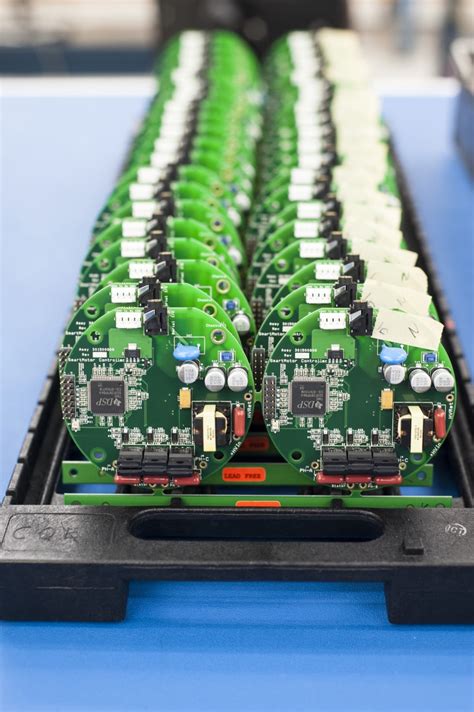
What is PCB Assembly?
PCB assembly is the process of assembling electronic components onto a printed circuit board (PCB) to create a functional electronic device. The PCB is a flat board made of insulating materials, such as fiberglass or plastic, with conductive pathways etched onto its surface. These pathways, known as traces, connect the various components on the board, allowing electrical signals to travel between them.
PCB assembly involves several steps, including:
- Solder paste application
- Component placement
- Soldering
- Inspection and testing
The assembled PCB is then integrated into the final electronic product, such as a smartphone, computer, or medical device.
Types of PCB Assembly
There are two main types of PCB assembly:
- Through-hole assembly (THA): Components with long leads are inserted through holes drilled in the PCB and soldered onto the opposite side.
- Surface-mount assembly (SMA): Components are placed directly onto the surface of the PCB and soldered in place.
| Assembly Type | Advantages | Disadvantages |
|---|---|---|
| Through-hole | – Stronger mechanical bonds – Easier to replace components – Better for high-power applications |
– Larger component size – Higher assembly costs – Slower assembly process |
| Surface-mount | – Smaller component size – Lower assembly costs – Faster assembly process – Higher component density |
– Weaker mechanical bonds – More difficult to replace components – Requires specialized equipment |
PCB Assembly Technology
Solder Paste Application
Solder paste, a mixture of tiny solder particles and flux, is applied to the PCB using a stencil or screen printing process. The stencil is a thin metal sheet with openings that correspond to the solder pad locations on the PCB. Solder paste is spread over the stencil, filling the openings and depositing the paste onto the pads.
Component Placement
Components are placed onto the solder paste-covered pads using pick-and-place machines. These machines use vacuum nozzles or grippers to pick up components from reels or trays and place them accurately on the PCB. Modern pick-and-place machines can place thousands of components per hour with high precision.
Soldering
After component placement, the PCB undergoes a soldering process to form electrical and mechanical connections between the components and the board. The most common Soldering Methods are:
- Reflow Soldering: The PCB is heated in an oven, causing the solder paste to melt and form connections between the components and the pads.
- Wave soldering: The PCB is passed over a molten solder wave, which selectively solders the through-hole components.
Inspection and Testing
After soldering, the assembled PCB undergoes inspection and testing to ensure proper functionality and quality. Common inspection methods include:
- Visual inspection: Manual or automated visual checks for component placement, solder joint quality, and other visible defects.
- Automated optical inspection (AOI): Uses cameras and image processing software to detect assembly defects.
- X-ray inspection: Uses X-rays to inspect solder joints and other internal features not visible from the surface.
Functional Testing may involve in-circuit testing (ICT), boundary scan testing, or functional test fixtures to verify the PCB’s performance and identify any defects.

Uses of PCB Assembly
PCB assembly is used in a wide range of industries and applications, including:
- Consumer electronics: Smartphones, tablets, laptops, TVs, and home appliances.
- Automotive: Engine control units, infotainment systems, sensors, and power management systems.
- Medical devices: Diagnostic equipment, monitoring systems, and implantable devices.
- Aerospace and defense: Avionics, communication systems, and military equipment.
- Industrial automation: Control systems, sensors, and robotics.

FAQ
1. What is the difference between PCB fabrication and PCB assembly?
PCB fabrication is the process of manufacturing the bare printed circuit board, which includes designing the circuit layout, etching the conductive pathways, and applying the protective coatings. PCB assembly is the process of populating the fabricated PCB with electronic components and soldering them in place to create a functional electronic assembly.
2. What are the advantages of surface-mount assembly over through-hole assembly?
Surface-mount assembly offers several advantages over through-hole assembly, including:
- Smaller component size, allowing for higher component density and more compact PCB designs.
- Lower assembly costs due to faster placement and soldering processes.
- Improved high-frequency performance due to reduced lead lengths and parasitic effects.
3. What is the purpose of solder paste in PCB assembly?
Solder paste serves two main purposes in PCB assembly:
- It provides a temporary adhesive to hold the components in place before soldering.
- It contains the solder alloy that forms the electrical and mechanical connections between the components and the PCB during the soldering process.
4. What are some common defects that can occur during PCB assembly?
Some common defects that can occur during PCB assembly include:
- Misaligned or missing components
- Solder bridging or insufficient solder joints
- Tombstoning (components standing on end due to uneven solder melting)
- Lifted or misaligned solder pads
- Contamination or foreign object debris (FOD)
5. How can PCB assembly quality be ensured?
PCB assembly quality can be ensured through a combination of:
- Proper design for manufacturability (DFM) practices
- Stringent process controls and standard operating procedures (SOPs)
- Regular equipment maintenance and calibration
- Skilled and well-trained operators
- Thorough inspection and testing at various stages of the assembly process
- Continuous improvement and root cause analysis of defects
By implementing these quality control measures, PCB assembly providers can consistently deliver high-quality, reliable electronic assemblies to their customers.


Leave a Reply