Introduction to PCB Assembly and Panel Requirements
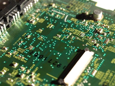
PCB (Printed Circuit Board) assembly is the process of soldering electronic components onto a printed circuit board to create a functional electronic device. The process involves several steps, including placing components on the board, soldering them in place, and testing the completed assembly to ensure proper functionality.
One of the critical aspects of PCB assembly is the panel requirements. A panel is a larger PCB that contains multiple smaller PCBs, which are separated after the assembly process. Panelization is used to increase production efficiency and reduce manufacturing costs by allowing multiple PCBs to be assembled simultaneously.
Key Considerations for Panel Requirements in PCB Assembly
When designing panels for PCB assembly, several key factors must be considered to ensure optimal results:
- Panel Size: The panel size should be compatible with the assembly equipment and maximize the number of PCBs per panel while minimizing waste.
- Panel Material: The panel material should be suitable for the assembly process and provide adequate support for the PCBs during handling and transport.
- Tooling Holes: Tooling holes are used to align the panel during the assembly process and should be positioned accurately to ensure proper registration.
- Fiducial Marks: Fiducial marks are used by assembly machines to align the panel and locate individual PCBs accurately. They should be clearly visible and positioned correctly.
- V-Scoring: V-scoring is a method of creating grooves in the panel to facilitate the separation of individual PCBs after assembly. The depth and angle of the V-score should be carefully calculated to ensure clean and accurate separation.
Panel Size and Material Selection
Determining the Optimal Panel Size
The panel size is a crucial factor in PCB assembly, as it directly impacts production efficiency and cost. When determining the optimal panel size, consider the following:
- Assembly Equipment Compatibility: Ensure that the panel size is compatible with the assembly equipment, including pick-and-place machines, reflow ovens, and inspection systems.
- PCB Dimensions: Consider the dimensions of the individual PCBs and determine the maximum number that can fit on a panel while leaving adequate space for tooling holes, fiducial marks, and v-scoring.
- Material Utilization: Aim to maximize material utilization by minimizing waste and optimizing the panel layout. This can be achieved by using a panel size that allows for efficient nesting of PCBs.
Choosing the Right Panel Material
The choice of panel material depends on several factors, including the assembly process, the end-use application, and the environmental conditions the PCBs will be exposed to. Common panel materials include:
- FR-4: FR-4 is a glass-reinforced epoxy laminate that is widely used in PCB Fabrication. It offers good mechanical and electrical properties, making it suitable for most applications.
- Aluminum: Aluminum panels are used in applications that require excellent heat dissipation, such as high-power electronics or LED lighting.
- Polyimide: Polyimide panels are used in applications that require high temperature resistance, such as aerospace or automotive electronics.
| Material | Advantages | Disadvantages |
|---|---|---|
| FR-4 | Good mechanical and electrical properties | Limited temperature resistance |
| Aluminum | Excellent heat dissipation | Higher cost and weight |
| Polyimide | High temperature resistance | Higher cost and limited availability |

Tooling Holes and Fiducial Marks
Positioning and Sizing of Tooling Holes
Tooling holes are essential for aligning the panel during the assembly process and ensuring accurate registration of the PCBs. When designing tooling holes, consider the following:
- Hole Diameter: The diameter of the tooling holes should be compatible with the assembly equipment and provide a secure fit for the tooling pins.
- Hole Placement: Tooling holes should be positioned accurately and consistently across the panel to ensure proper alignment. They should be located near the corners of the panel and evenly spaced along the edges.
- Hole-to-Hole Distance: The distance between tooling holes should be consistent and within the specifications of the assembly equipment to prevent misalignment or panel warpage.
Fiducial Mark Design and Placement
Fiducial marks are used by assembly machines to locate and align individual PCBs on the panel. They are typically small, circular features that are placed at specific locations on the panel. When designing fiducial marks, consider the following:
- Mark Size: Fiducial marks should be large enough to be easily detected by the assembly machines but small enough to minimize their impact on the PCB Design.
- Mark Placement: Fiducial marks should be placed at the corners of each PCB on the panel and should be positioned accurately to ensure proper alignment.
- Mark Contrast: Fiducial marks should have high contrast against the panel background to facilitate accurate detection by the assembly machines. This can be achieved by using a copper or soldermask finish that contrasts with the panel material.
| Fiducial Mark Placement | Advantages | Disadvantages |
|---|---|---|
| Corners of each PCB | Accurate alignment of individual PCBs | May interfere with PCB design |
| Panel corners | Minimizes impact on PCB design | Less accurate alignment of individual PCBs |

V-Scoring and Panel Separation
Designing V-Scores for Clean PCB Separation
V-scoring is a method of creating grooves in the panel to facilitate the separation of individual PCBs after assembly. When designing v-scores, consider the following:
- V-Score Depth: The depth of the v-score should be carefully calculated to ensure that it is deep enough to allow for clean separation of the PCBs but not so deep that it compromises the structural integrity of the panel during assembly.
- V-Score Angle: The angle of the v-score should be chosen to minimize stress on the PCBs during separation. A typical v-score angle is 30 degrees, but this may vary depending on the panel material and thickness.
- V-Score Placement: V-scores should be placed along the edges of each PCB on the panel, leaving adequate space for tooling holes and fiducial marks.
Separating PCBs from the Panel
After the assembly process is complete, the individual PCBs must be separated from the panel. This can be done manually or using automated equipment, depending on the production volume and requirements. When separating PCBs from the panel, consider the following:
- Separation Method: Manual separation using hand tools or automated separation using a depaneling machine should be chosen based on the production volume, panel material, and v-score design.
- Handling and Transport: Separated PCBs should be handled and transported carefully to avoid damage. The use of ESD (Electrostatic Discharge) protection measures, such as grounded wrist straps and ESD-safe packaging, is recommended.
| Separation Method | Advantages | Disadvantages |
|---|---|---|
| Manual | Low cost | Time-consuming and prone to human error |
| Automated | High speed and consistency | Higher equipment cost and setup time |

Conclusion
Panel requirements play a critical role in the success of PCB assembly projects. By carefully considering factors such as panel size, material selection, tooling holes, fiducial marks, and v-scoring, designers can ensure that their PCBs are manufactured efficiently and with high quality.
Effective communication between the PCB design team and the assembly provider is essential to ensure that panel requirements are understood and implemented correctly. By working together and following best practices, designers and assemblers can achieve optimal results and bring innovative electronic products to market quickly and cost-effectively.
Frequently Asked Questions (FAQ)
-
What is the purpose of panelization in PCB assembly?
Panelization is used to increase production efficiency and reduce manufacturing costs by allowing multiple PCBs to be assembled simultaneously on a single panel. -
How do I determine the optimal panel size for my PCB design?
When determining the optimal panel size, consider the compatibility with assembly equipment, the dimensions of the individual PCBs, and the goal of maximizing material utilization while minimizing waste. -
What are the most common panel materials used in PCB assembly?
Common panel materials include FR-4, a glass-reinforced epoxy laminate suitable for most applications; aluminum, which offers excellent heat dissipation; and polyimide, which provides high temperature resistance. -
Why are fiducial marks important in PCB assembly?
Fiducial marks are used by assembly machines to locate and align individual PCBs on the panel accurately. They ensure proper registration and help maintain consistent quality throughout the assembly process. -
What is the purpose of v-scoring in PCB Panelization?
V-scoring creates grooves in the panel that facilitate the clean separation of individual PCBs after the assembly process is complete. The depth and angle of the v-score must be carefully designed to ensure optimal results.


Leave a Reply