What is PCB Panelization?
PCB panelization involves arranging multiple identical or different PCB designs on a single larger board, known as a panel. This allows for bulk production of PCBs in a single manufacturing run, reducing setup time and costs. Panels are designed to fit the specific dimensions of the manufacturing equipment and typically include additional features such as tooling holes, fiducial markers, and breakaway tabs to aid in the fabrication and assembly process.
Benefits of PCB Panelization
-
Cost reduction: Panelizing PCBs minimizes the number of manufacturing runs required, reducing setup costs and material waste.
-
Increased efficiency: Producing multiple PCBs on a single panel streamlines the fabrication process, allowing for faster turnaround times.
-
Improved quality: Consistent panel design ensures uniform processing conditions for all PCBs, resulting in higher quality and reliability.
-
Simplified handling: Panels are easier to handle and transport than individual PCBs, reducing the risk of damage during manufacturing and assembly.
Preparing Your PCB Design for Panelization
Before you begin the panelization process, it’s essential to ensure your PCB design is optimized for manufacturing. Follow these guidelines to prepare your design:
Design Rules Check (DRC)
Perform a thorough Design Rules Check (DRC) on your PCB Layout to identify and resolve any potential issues, such as insufficient clearances, incorrect trace widths, or missing Solder Mask openings. Consult your manufacturer’s design guidelines to ensure compatibility with their fabrication capabilities.
Gerber Files Generation
Export your PCB design as a set of Gerber files, which are industry-standard file formats used for PCB Fabrication. Ensure that all necessary layers are included, such as top and bottom copper, solder mask, silkscreen, and drill files. Verify the accuracy of your Gerber files using a Gerber viewer to catch any errors before proceeding with panelization.
Panel Size and Orientation
Determine the optimal panel size and orientation based on your PCB dimensions and the manufacturer’s equipment specifications. Consider factors such as the number of PCBs per panel, the spacing between individual boards, and the placement of tooling holes and fiducial markers. Aim to maximize the panel utilization while ensuring sufficient spacing for depanelization and assembly.

Using CAM Software for PCB Panelization
CAM software provides the tools and features necessary to create efficient and reliable PCB panels. Popular CAM software options include Altium Designer, Cadence Allegro, and Mentor Graphics Xpedition. Follow these steps to panelize your PCBs using CAM software:
Step 1: Import PCB Design
Import your PCB design into the CAM software, either as a complete layout or individual Gerber files. Ensure that all layers are correctly aligned and positioned relative to the origin point.
Step 2: Define Panel Dimensions
Set the panel dimensions based on your predetermined panel size and the manufacturer’s specifications. Consider the maximum and minimum panel sizes allowed by the fabrication equipment.
Step 3: Arrange PCBs on Panel
Place your PCB designs on the panel, taking into account the required spacing between boards and the panel edges. Use the CAM software’s array tools to create a grid of identical PCBs or manually position different designs as needed. Ensure consistent orientation and alignment of all boards.
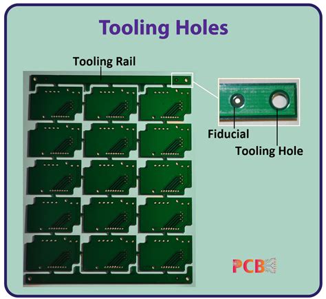
Step 4: Add Tooling Holes and Fiducial Markers
Include tooling holes and fiducial markers on the panel to aid in the fabrication and assembly process. Tooling holes are used to secure the panel during drilling and routing, while fiducial markers serve as reference points for automated assembly equipment. Place these features in accordance with your manufacturer’s guidelines.
Step 5: Create Breakaway Tabs
Design breakaway tabs or mousebites along the edges of individual PCBs to facilitate depanelization. These tabs connect the boards to the panel frame and are removed after fabrication, allowing for easy separation of individual PCBs. Ensure that the tab size and spacing are appropriate for your PCB Thickness and manufacturing process.
Step 6: Generate Manufacturing Files
Once your panel design is complete, generate the necessary manufacturing files, including the updated Gerber files and drill files. Perform a final check to ensure all layers are correctly aligned and the panel dimensions meet the manufacturer’s requirements.

Best Practices for PCB Panelization
To achieve optimal results when panelizing your PCBs, consider the following best practices:
-
Minimize waste: Optimize panel utilization by arranging PCBs efficiently and minimizing unused space.
-
Maintain consistent orientation: Ensure all PCBs on the panel have the same orientation to simplify assembly and reduce errors.
-
Allow for depanelization: Provide sufficient spacing between individual boards and the panel frame to accommodate depanelization methods, such as routing or punching.
-
Consider assembly requirements: Take into account the assembly process when designing your panel, ensuring adequate clearance for pick-and-place machines and other equipment.
-
Communicate with your manufacturer: Work closely with your PCB manufacturer to ensure your panel design meets their specific requirements and capabilities.

Common Challenges and Solutions
During the PCB panelization process, you may encounter various challenges. Here are some common issues and their solutions:
Issue 1: Insufficient spacing between boards
If the spacing between individual PCBs is too tight, it can lead to manufacturing difficulties and potential damage during depanelization.
Solution: Increase the spacing between boards to provide adequate room for fabrication tolerances and depanelization methods. Consult your manufacturer’s guidelines for recommended spacing values.
Issue 2: Incorrect fiducial marker placement
Improperly placed fiducial markers can cause alignment issues during automated assembly, resulting in component misplacement or soldering defects.
Solution: Ensure fiducial markers are placed in accordance with the manufacturer’s specifications and industry standards. Use a minimum of three fiducial markers per panel, positioned at the corners or edges of the panel.
Issue 3: Inadequate tab strength
If the breakaway tabs or mousebites are too small or weak, they may break prematurely during handling or transport, causing damage to the individual PCBs.
Solution: Design breakaway tabs with appropriate size and spacing based on your PCB thickness and material. Use a minimum of two tabs per edge, and consider adding additional tabs for larger or heavier boards.
FAQ
- Can I panelize PCBs with different designs on the same panel?
Yes, it is possible to panelize different PCB designs on a single panel, known as a mixed panel. However, it’s essential to ensure that all designs have the same thickness, material, and finishing requirements to avoid manufacturing complications.
- How do I determine the optimal panel size for my PCBs?
The optimal panel size depends on various factors, such as the dimensions of your individual PCBs, the manufacturer’s equipment specifications, and the desired number of boards per panel. Consult with your manufacturer to determine the most suitable panel size for your specific project.
- What is the minimum spacing required between individual PCBs on a panel?
The minimum spacing between PCBs on a panel varies depending on the manufacturing process and the depanelization method used. Generally, a minimum spacing of 2-3 mm is recommended, but it’s always best to consult your manufacturer’s guidelines for specific requirements.
- Can I panelize PCBs with different copper thicknesses?
It’s not recommended to panelize PCBs with different copper thicknesses on the same panel, as this can lead to uneven etching and potential manufacturing issues. If you need to panelize PCBs with varying copper thicknesses, it’s best to create separate panels for each thickness.
- How do I ensure my PCB design is compatible with the panelization process?
To ensure compatibility with the panelization process, follow your manufacturer’s design guidelines and adhere to industry standards. Perform thorough Design Rules Checks (DRC) on your PCB layout, generate accurate Gerber files, and communicate regularly with your manufacturer to address any potential issues.
| Panel Size | Number of PCBs | Spacing Between PCBs |
|---|---|---|
| 200 mm x 150 mm | 4 | 3 mm |
| 250 mm x 200 mm | 6 | 2.5 mm |
| 300 mm x 250 mm | 9 | 2 mm |
By following the guidelines and best practices outlined in this article, you can successfully panelize your PCBs using CAM software, ensuring efficient and cost-effective manufacturing. Remember to work closely with your PCB manufacturer throughout the process to address any challenges and ensure the best possible results for your project.


Leave a Reply