Introduction to PCB Thickness
Printed circuit board (PCB) thickness is a critical factor in the design and manufacture of electronic devices. The thickness of a PCB can affect its mechanical strength, electrical performance, thermal management, and overall reliability. In this article, we will explore the various aspects of PCB thickness, including the standard thicknesses, factors influencing thickness selection, manufacturing considerations, and frequently asked questions.
Standard PCB Thicknesses
PCBs come in a range of standard thicknesses, measured in either inches or millimeters. The most common PCB thicknesses are:
| Thickness (Inches) | Thickness (Millimeters) |
|---|---|
| 0.012″ | 0.31 mm |
| 0.016″ | 0.41 mm |
| 0.020″ | 0.51 mm |
| 0.024″ | 0.61 mm |
| 0.031″ | 0.79 mm |
| 0.039″ | 0.99 mm |
| 0.047″ | 1.19 mm |
| 0.062″ | 1.57 mm |
| 0.093″ | 2.36 mm |
| 0.125″ | 3.18 mm |
These standard thicknesses are derived from the available copper foil weights and the number of layers in the PCB Stack-Up. The choice of PCB thickness depends on various factors, which we will discuss in the following sections.

Factors Influencing PCB Thickness Selection
1. Number of Layers
The number of layers in a PCB is one of the primary factors determining its thickness. As the number of layers increases, so does the overall thickness of the board. The relationship between the number of layers and PCB thickness can be summarized as follows:
| Number of Layers | Typical Thickness Range (mm) |
|---|---|
| 1 | 0.2 – 0.4 |
| 2 | 0.4 – 0.8 |
| 4 | 0.8 – 1.6 |
| 6 | 1.2 – 2.4 |
| 8 | 1.6 – 3.2 |
| 10+ | 2.0 – 4.0+ |
Single-layer and double-layer PCBs are typically thinner, while multi-layer boards with four or more layers are thicker to accommodate the additional copper layers and insulation.
2. Copper Thickness
The thickness of the copper foil used in PCB manufacturing also contributes to the overall board thickness. Copper thickness is measured in ounces per square foot (oz/ft²), with common values ranging from 0.5 oz/ft² to 3 oz/ft². The relationship between copper thickness and PCB thickness is as follows:
| Copper Thickness (oz/ft²) | Copper Thickness (µm) | PCB Thickness Contribution (mm) |
|---|---|---|
| 0.5 | 17.5 | 0.018 |
| 1 | 35 | 0.035 |
| 2 | 70 | 0.070 |
| 3 | 105 | 0.105 |
Thicker copper foils are used for high-current applications or to improve thermal management, but they also increase the overall PCB thickness.
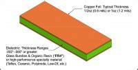
3. Substrate Material
The choice of substrate material also affects PCB thickness. The most common substrate materials are:
- FR-4: A glass-reinforced epoxy laminate, widely used for its good mechanical and electrical properties.
- Rogers Materials: High-frequency laminates with low dielectric loss, used in RF and microwave applications.
- Polyimide: A high-temperature, flexible substrate material used in aerospace and military applications.
Each substrate material has its own dielectric thickness, which contributes to the overall PCB thickness. For example, standard FR-4 laminates have a thickness of 0.1 mm to 3.2 mm, while Rogers materials can range from 0.127 mm to 1.57 mm.
4. Application Requirements
The specific requirements of the end application also influence PCB thickness selection. Some key considerations include:
- Mechanical Strength: Thicker PCBs offer better mechanical strength and rigidity, which is important for applications subject to vibration, shock, or physical stress.
- Electrical Performance: The PCB thickness can affect signal integrity, impedance control, and crosstalk. Thinner boards are often preferred for high-speed digital designs to minimize signal distortion.
- Thermal Management: Thicker PCBs with heavier copper layers can improve heat dissipation, which is crucial for power electronics and high-temperature applications.
- Space Constraints: In space-limited applications, such as mobile devices or wearables, thinner PCBs are favored to reduce the overall device thickness.
Designers must balance these requirements and constraints to select the appropriate PCB thickness for their specific application.

Manufacturing Considerations
1. Aspect Ratio
The aspect ratio is the ratio of the PCB thickness to the smallest drill diameter. It is an important consideration in PCB manufacturing, as it affects the ease and reliability of drilling and plating processes. A higher aspect ratio (thicker board with smaller drill diameters) increases the complexity and cost of manufacturing. The recommended aspect ratio for reliable PCB production is 8:1 or less.
2. Plating and Vias
The PCB thickness also affects the plating process, particularly for through-hole vias. Thicker boards require longer plating times to ensure proper copper coverage in the via holes. This can lead to increased manufacturing time and cost. Additionally, thicker boards may require larger via diameters to maintain a manageable aspect ratio, which can impact routing density.
3. Lamination and Warping
During the lamination process, thicker PCBs are more prone to warping due to the increased number of layers and the greater amount of heat and pressure applied. Warping can cause issues with component assembly and solder joint reliability. To mitigate warping, manufacturers may employ techniques such as balanced stack-ups, symmetrical copper distribution, and controlled heating and cooling cycles.

Frequently Asked Questions (FAQ)
1. What is the most common PCB thickness?
The most common PCB thickness is 1.6 mm (0.062″), as it offers a good balance between mechanical strength, electrical performance, and manufacturing ease. This thickness is widely used in consumer electronics, industrial controls, and general-purpose applications.
2. Can I use a thinner PCB to reduce costs?
While thinner PCBs may have a lower material cost, they can actually increase overall costs due to manufacturing challenges and reduced yields. Thinner boards are more prone to warping, handling damage, and assembly issues, which can lead to higher scrap rates and rework costs. It is essential to consider the total cost impact when selecting a PCB thickness.
3. How does PCB thickness affect impedance control?
PCB thickness is one of the factors that influence impedance control in high-speed designs. Thinner dielectric layers between copper traces result in higher characteristic impedance, while thicker dielectrics lead to lower impedance. Designers must carefully select the appropriate PCB thickness and layer stack-up to achieve the desired impedance targets and maintain signal integrity.
4. Can I mix different PCB thicknesses in the same design?
Yes, it is possible to have different PCB thicknesses within the same design, known as a “rigid-flex” or “multi-stage” PCB. This approach combines rigid and flexible PCB sections, allowing for improved packaging density and mechanical flexibility. However, designing and manufacturing Rigid-flex PCBs is more complex and costly compared to standard rigid PCBs.
5. How do I choose the right PCB thickness for my application?
Choosing the right PCB thickness involves considering multiple factors, such as the number of layers, copper thickness, substrate material, and application requirements. It is essential to consult with experienced PCB designers and manufacturers to determine the optimal thickness for your specific application. They can help you balance the trade-offs between mechanical, electrical, thermal, and manufacturing considerations to achieve the best overall performance and cost-effectiveness.
Conclusion
PCB thickness is a critical aspect of electronic design and manufacturing, with far-reaching implications for mechanical strength, electrical performance, thermal management, and reliability. By understanding the factors influencing PCB thickness selection, such as the number of layers, copper thickness, substrate material, and application requirements, designers can make informed decisions to optimize their PCB designs.
However, PCB thickness also presents manufacturing challenges, including aspect ratio limitations, plating and via considerations, and warping issues during lamination. Working closely with experienced PCB manufacturers and following best design practices can help mitigate these challenges and ensure successful PCB production.
As electronic devices continue to push the boundaries of performance, miniaturization, and functionality, the story of PCB thickness remains complex and ever-evolving. By staying informed about the latest advancements in materials, manufacturing processes, and design techniques, engineers and manufacturers can innovate and adapt to meet the demands of the rapidly changing electronics landscape.


Leave a Reply