What is PCB Fabrication?
PCB fabrication is the process of creating a printed circuit board from a digital design file. It involves a series of steps that transform a bare substrate material, typically a copper-clad laminate, into a functional PCB with conductive traces, pads, and other features. The fabrication process ensures that the PCB meets the specified design requirements, such as signal integrity, power distribution, and mechanical stability.
The PCB Fabrication Process
The PCB fabrication process can be divided into several key stages, each contributing to the final quality and functionality of the board. Let’s explore each stage in detail.
1. PCB Design and Preparation
The PCB fabrication journey begins with the design phase. Using specialized PCB design software, engineers create a digital representation of the circuit, specifying the layout, component placement, and interconnections. The design is then reviewed and optimized to ensure manufacturability and adherence to industry standards.
Once the design is finalized, it is converted into a set of fabrication files, typically in the Gerber format. These files contain the necessary information for each layer of the PCB, including the copper traces, solder mask, silkscreen, and drill holes.
2. Substrate Preparation
The substrate, usually a copper-clad laminate, serves as the foundation of the PCB. The most common substrate materials are FR-4 (a glass-reinforced epoxy laminate) and Rogers (a high-frequency laminate). The substrate is cut to the desired size and shape using precise cutting machines.
3. Copper Patterning
The next step is to transfer the copper pattern from the design files onto the substrate. This is typically achieved through a photolithography process. Here’s how it works:
- The substrate is cleaned and dried to ensure a pristine surface.
- A photoresist layer, a light-sensitive material, is applied evenly onto the copper surface.
- The photoresist is exposed to UV light through a photomask, which contains the desired copper pattern.
- The exposed areas of the photoresist harden, while the unexposed areas remain soluble.
- The substrate is developed, removing the soluble photoresist and revealing the copper pattern.
- The exposed copper is etched away using a chemical solution, leaving only the desired copper traces.
4. Drilling
After the copper patterning, the PCB undergoes a drilling process to create the necessary holes for through-hole components and vias. High-speed drilling machines accurately drill the holes based on the drill file generated from the PCB design software. The holes are then cleaned and deburred to ensure smooth and reliable connections.
5. Plating and Coating
To enhance the conductivity and durability of the PCB, various plating and coating processes are applied. These include:
- Electroless copper plating: A thin layer of copper is deposited onto the drilled holes and exposed copper surfaces to improve conductivity and prevent oxidation.
- Electrolytic copper plating: A thicker layer of copper is electroplated onto the PCB to increase the thickness of the copper traces and provide better current-carrying capacity.
- Solder mask application: A protective solder mask layer is applied to the PCB, covering the copper traces while leaving the pads and other designated areas exposed. This prevents short circuits and enhances the aesthetic appeal of the board.
- Silkscreen printing: Text, symbols, and component identifiers are printed onto the PCB using a silkscreen process, aiding in assembly and troubleshooting.
6. Surface Finish
The exposed copper pads and other areas of the PCB require a surface finish to protect them from oxidation and enhance solderability. Common surface finishes include:
- Hot Air Solder Leveling (HASL): A thin layer of solder is applied to the exposed copper areas using a hot air leveling process.
- Immersion Silver (IAg): A thin layer of silver is chemically deposited onto the exposed copper surfaces.
- Electroless Nickel Immersion Gold (ENIG): A layer of nickel is first deposited, followed by a thin layer of gold, providing excellent solderability and corrosion resistance.
- Immersion Tin (ISn): A thin layer of tin is chemically deposited onto the exposed copper areas, offering good solderability and affordability.
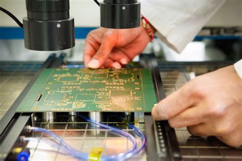
7. Electrical Testing
Before the PCB is considered complete, it undergoes rigorous electrical testing to ensure its functionality and reliability. Automated testing equipment, such as flying probe testers or bed-of-nails fixtures, checks for continuity, short circuits, and open circuits. This step helps identify any manufacturing defects or design issues that may affect the PCB’s performance.
8. Final Inspection and Packaging
After passing the electrical tests, the PCBs undergo a final visual inspection to check for any cosmetic defects, such as scratches, dents, or discolorations. Once the PCBs are deemed satisfactory, they are packaged and shipped to the customer or sent for assembly.

PCB Assembly
While PCB fabrication focuses on creating the bare PCB, PCB assembly involves populating the board with electronic components. The assembly process can be categorized into two main types:
- Through-hole assembly: Components with long leads are inserted into drilled holes on the PCB and soldered onto the opposite side.
- Surface-mount assembly: Components with small leads or terminations are placed directly onto the PCB’s surface and soldered using reflow or wave soldering techniques.
PCB assembly can be done manually for low-volume production or prototyping, but automated assembly lines are used for high-volume manufacturing to ensure speed, accuracy, and consistency.

PCB Fabrication Considerations
When designing and fabricating PCBs, several key factors should be considered to ensure optimal performance and manufacturability:
- Material selection: Choose the appropriate substrate material based on the application’s requirements, such as dielectric constant, thermal stability, and cost.
- Layer stackup: Determine the number of layers and their arrangement to accommodate the circuit complexity, signal integrity, and power distribution needs.
- Trace width and spacing: Ensure that the trace widths and spacing meet the manufacturing capabilities and design rules to avoid signal integrity issues and manufacturing defects.
- Via placement: Optimize the placement and size of vias to minimize signal reflections, crosstalk, and manufacturing challenges.
- Thermal management: Consider the thermal dissipation requirements of the components and design appropriate copper areas, thermal vias, or heatsinks to prevent overheating.
- Electromagnetic compatibility (EMC): Implement EMC design techniques, such as proper grounding, shielding, and filtering, to minimize electromagnetic interference (EMI) and ensure compliance with regulatory standards.

PCB Fabrication Standards and Certifications
To ensure the quality and reliability of PCBs, various industry standards and certifications have been established. Some of the key standards include:
- IPC (Association Connecting Electronics Industries) standards:
- IPC-A-600: Acceptability of Printed Boards
- IPC-6012: Qualification and Performance Specification for Rigid Printed Boards
- IPC-2221: Generic Standard on Printed Board Design
- UL (Underwriters Laboratories) standards:
- UL 94: Standard for Safety of Flammability of Plastic Materials
- UL 796: Standard for Safety of Printed Wiring Boards
- RoHS (Restriction of Hazardous Substances) Directive: Regulates the use of hazardous substances in electronic and electrical products.
Ensuring compliance with these standards helps maintain the quality, safety, and environmental friendliness of PCBs.
Choosing a PCB Fabrication Partner
Selecting the right PCB fabrication partner is crucial for the success of your project. Consider the following factors when evaluating potential fabricators:
- Capabilities: Ensure that the fabricator has the necessary equipment, expertise, and experience to handle your specific PCB requirements, such as layer count, material, and feature sizes.
- Quality control: Look for fabricators with robust quality control processes, including automated optical inspection (AOI), X-ray inspection, and electrical testing, to ensure consistent and reliable PCBs.
- Certifications: Choose a fabricator that holds relevant certifications, such as ISO 9001 (quality management) and ISO 14001 (environmental management), to demonstrate their commitment to quality and sustainability.
- Lead time and pricing: Consider the fabricator’s lead time and pricing structure to ensure they align with your project timeline and budget.
- Customer support: Evaluate the fabricator’s responsiveness, communication, and technical support to ensure a smooth collaboration throughout the fabrication process.
By carefully selecting a reputable and experienced PCB fabrication partner, you can minimize risks, ensure timely delivery, and achieve the desired quality for your PCBs.
FAQ
- What is the typical turnaround time for PCB fabrication?
-
The turnaround time for PCB fabrication varies depending on the complexity of the design, the fabricator’s workload, and the chosen service level. Standard lead times range from 5 to 15 business days, while expedited services can provide faster turnaround times at an additional cost.
-
Can I fabricate PCBs with multiple layers?
-
Yes, PCBs can be fabricated with multiple layers, ranging from single-layer to multi-layer boards with 8, 12, or even more layers. The number of layers depends on the complexity of the circuit, the signal integrity requirements, and the available space for routing.
-
What is the minimum feature size achievable in PCB fabrication?
-
The minimum feature size, such as trace width and spacing, depends on the fabricator’s capabilities and the chosen manufacturing process. Typical minimum feature sizes range from 3 to 6 mils (0.075 to 0.15 mm) for standard PCB fabrication, while advanced processes can achieve even smaller features.
-
How can I ensure the manufacturability of my PCB design?
-
To ensure the manufacturability of your PCB design, follow the fabricator’s design guidelines, which specify the minimum feature sizes, clearances, and other design rules. Perform design rule checks (DRC) using your PCB design software to identify and resolve any violations. Additionally, consult with your fabricator early in the design process to discuss any specific requirements or limitations.
-
What is the difference between PCB fabrication and PCB assembly?
- PCB fabrication refers to the process of creating the bare PCB, which includes the substrate, copper traces, solder mask, and silkscreen. PCB assembly, on the other hand, involves populating the fabricated PCB with electronic components, such as resistors, capacitors, and integrated circuits, using through-hole or surface-mount techniques.
Conclusion
PCB fabrication is a complex and multi-faceted process that transforms a digital design into a functional printed circuit board. By understanding the various stages involved, from design and substrate preparation to copper patterning, plating, and testing, you can make informed decisions and optimize your PCB design for manufacturability and performance.
When embarking on a PCB fabrication project, consider factors such as material selection, layer stackup, trace width and spacing, and thermal management to ensure the best possible outcomes. Adhere to industry standards and certifications to maintain quality and reliability.
Choosing the right PCB fabrication partner is equally important. Evaluate their capabilities, quality control processes, certifications, lead times, pricing, and customer support to find a fabricator that aligns with your project requirements and expectations.
By demystifying the PCB fabrication process and following best practices, you can successfully bring your electronic designs to life, creating reliable and efficient PCBs that power the devices and systems of today and tomorrow.
| PCB Fabrication Process | Description |
|---|---|
| Design and Preparation | Create digital design, generate fabrication files (Gerber) |
| Substrate Preparation | Cut copper-clad laminate to desired size and shape |
| Copper Patterning | Transfer copper pattern using photolithography and etching |
| Drilling | Create holes for through-hole components and vias |
| Plating and Coating | Apply electroless copper plating, electrolytic copper plating, solder mask, and silkscreen |
| Surface Finish | Protect exposed copper areas with HASL, IAg, ENIG, or ISn |
| Electrical Testing | Perform continuity, short circuit, and open circuit tests |
| Final Inspection | Check for cosmetic defects and package for shipping or assembly |


Leave a Reply