Introduction to Solder Mask
Solder mask, also known as solder resist or solder stop mask, is a thin layer of polymer that is applied to the surface of a printed circuit board (PCB) to protect the copper traces from oxidation, contamination, and accidental solder bridging during the assembly process. This protective layer is a crucial component in the manufacturing of PCBs, as it ensures the proper functioning and reliability of the electronic devices in which they are used.
What is a Printed Circuit Board (PCB)?
A printed circuit board is a flat board made of insulating materials, such as fiberglass or composite epoxy, with conductive copper traces etched onto its surface. These copper traces form the electrical connections between various components, such as resistors, capacitors, and integrated circuits (ICs), which are soldered onto the board. PCBs are used in almost all electronic devices, from smartphones and computers to automobiles and aerospace equipment.
The Role of Solder Mask in PCB Manufacturing
Solder mask plays a vital role in the PCB manufacturing process by providing several key benefits:
-
Protection from oxidation: Copper traces on a PCB can easily oxidize when exposed to air, leading to reduced conductivity and potential electrical failures. Solder mask acts as a barrier, preventing the copper from oxidizing and maintaining its conductivity.
-
Prevention of solder bridging: During the soldering process, molten solder can accidentally flow between adjacent copper traces, causing short circuits known as solder bridges. Solder mask covers the areas between the traces, preventing solder from adhering to unintended locations and minimizing the risk of solder bridging.
-
Insulation: Solder mask acts as an insulating layer, preventing accidental contact between components and copper traces, which can lead to electrical shorts or damage to the components.
-
Improved aesthetics: Solder mask is available in various colors, with green being the most common. The colored surface of the PCB enhances its visual appearance and makes it easier to inspect for defects or damage.
Types of Solder Mask
There are two main types of solder mask used in PCB manufacturing: liquid photoimageable solder mask (LPISM) and dry film solder mask (DFSM).
Liquid Photoimageable Solder Mask (LPISM)
LPISM is the most commonly used type of solder mask in the PCB industry. It is applied to the PCB surface as a liquid polymer and then exposed to ultraviolet (UV) light through a photomask. The areas of the solder mask that are exposed to UV light cure and harden, while the unexposed areas remain liquid and can be easily removed during the development process.
Advantages of LPISM:
– High resolution and accuracy
– Excellent adhesion to the PCB surface
– Suitable for fine-pitch components and high-density designs
– Available in various colors and finishes (matte, glossy, or semi-glossy)
Disadvantages of LPISM:
– Requires a clean room environment for application
– Longer processing time compared to DFSM
– Higher cost than DFSM
Dry Film Solder Mask (DFSM)
DFSM is a solid photopolymer film that is laminated onto the PCB surface using heat and pressure. Like LPISM, it is exposed to UV light through a photomask, and the unexposed areas are removed during the development process.
Advantages of DFSM:
– Faster processing time compared to LPISM
– Lower cost than LPISM
– Suitable for high-volume production
Disadvantages of DFSM:
– Lower resolution and accuracy compared to LPISM
– Limited color options (usually green or purple)
– May not adhere well to uneven PCB surfaces

Solder Mask Application Process
The solder mask application process involves several steps to ensure proper coverage and adhesion to the PCB surface.
Step 1: Surface Preparation
Before applying the solder mask, the PCB surface must be thoroughly cleaned to remove any contaminants, such as dirt, grease, or oxidation. This is typically done using a combination of mechanical and chemical cleaning methods, such as brushing, scrubbing, and dipping the PCB in cleaning solutions.
Step 2: Solder Mask Application
The method of solder mask application depends on the type of solder mask being used.
For LPISM:
1. The liquid solder mask is applied to the PCB surface using a screen printing or spraying technique.
2. The PCB is then prebaked to remove any solvents and improve the solder mask’s adhesion to the surface.
For DFSM:
1. The dry film is laminated onto the PCB surface using heat and pressure.
2. The laminated PCB is then allowed to cool and stabilize.
Step 3: Exposure and Development
- The PCB with the applied solder mask is placed in an exposure machine, where it is exposed to UV light through a photomask. The photomask contains the desired solder mask pattern, allowing UV light to pass through only in specific areas.
- After exposure, the PCB undergoes a development process, where the unexposed areas of the solder mask are removed using a chemical developer solution.
Step 4: Curing
The PCB is then placed in an oven for the final curing process, where the solder mask is heated to a specific temperature for a set duration. This process ensures that the solder mask is fully hardened and properly adhered to the PCB surface.
Step 5: Inspection and Quality Control
After the curing process, the PCB is inspected for any defects or irregularities in the solder mask coverage. Common inspection methods include:
- Visual inspection: Checking for any visible defects, such as pinholes, blisters, or uneven coverage
- Thickness measurement: Verifying that the solder mask thickness is within the specified range
- Adhesion testing: Ensuring that the solder mask is properly adhered to the PCB surface
PCBs that pass the inspection process are then ready for the next stages of the manufacturing process, such as component assembly and soldering.

Solder Mask Design Considerations
When designing a PCB, several factors must be considered to ensure proper solder mask application and performance.
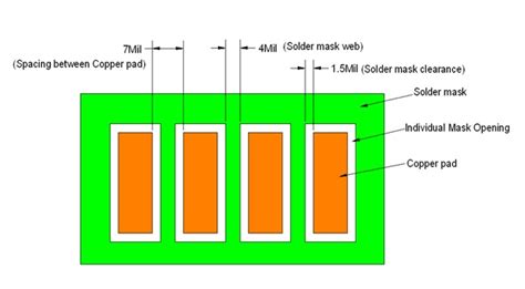
Solder Mask Clearance
Solder mask clearance refers to the space between the edge of the copper pad and the opening in the solder mask. This space allows for proper solder wetting during the assembly process and accommodates any misalignment between the solder mask and the copper pads.
The recommended solder mask clearance varies depending on the PCB design and manufacturing capabilities, but a general guideline is to have a clearance of 0.05 mm to 0.1 mm (2 to 4 mils) around the copper pads.
Solder Mask Sliver
A solder mask sliver is a thin strip of solder mask between two adjacent copper pads or traces. If the sliver is too thin, it may break away during the manufacturing process or fail to provide adequate insulation between the pads.
To prevent solder mask slivers, designers should maintain a minimum solder mask width between adjacent pads. The minimum width depends on the PCB manufacturer’s capabilities, but a common guideline is to keep the solder mask width greater than 0.1 mm (4 mils).
Solder Mask Color Selection
While green is the most common solder mask color, other colors such as red, blue, yellow, black, and white are also available. The choice of solder mask color can be based on several factors:
- Aesthetics: The color of the solder mask can contribute to the overall visual appeal of the PCB.
- Contrast: Choosing a solder mask color that contrasts well with the component markings and silkscreen can improve readability and ease of inspection.
- UV resistance: Some solder mask colors, such as black and white, offer better resistance to UV light, which can be important for PCBs used in outdoor applications.
- Thermal properties: Different solder mask colors may have slightly different thermal properties, which can affect heat dissipation in high-power applications.

Solder Mask Performance Standards
Several industry standards govern the performance and testing of solder masks to ensure their quality and reliability.
IPC-SM-840E
IPC-SM-840E is a standard developed by the IPC (Association Connecting Electronics Industries) that covers the qualification and performance of permanent solder mask. This standard defines the requirements for solder mask properties such as:
- Adhesion
- Resistance to solvents and chemicals
- Dielectric strength
- Flammability
- Thermal shock resistance
PCB manufacturers use this standard to ensure that their solder mask materials and processes meet the required performance criteria.
UL 94
UL 94 is a flammability standard developed by Underwriters Laboratories (UL) that classifies materials based on their burning characteristics. Solder masks are typically rated as V-0, which means that the material self-extinguishes within 10 seconds after removing the flame, and no flaming drips are allowed.
Having a UL 94 V-0 rating is important for PCBs used in applications where fire safety is a concern, such as consumer electronics and automotive systems.
Common Solder Mask Defects and Troubleshooting
During the solder mask application process, various defects can occur that may affect the PCB’s performance or reliability. Some common solder mask defects include:
Pinholes
Pinholes are small holes or voids in the solder mask that expose the underlying copper. These defects can be caused by:
- Contamination on the PCB surface before solder mask application
- Improper solder mask application or curing
- Trapped air bubbles during the application process
Pinholes can lead to solder bridging, corrosion, or short circuits. To prevent pinholes, ensure that the PCB surface is thoroughly cleaned before solder mask application and that the application process is optimized to minimize air entrapment.
Blisters
Blisters are raised areas of solder mask that can occur due to:
- Moisture trapped beneath the solder mask during the curing process
- Incompatibility between the solder mask and the PCB surface material
- Excessive curing temperatures
Blisters can cause solder mask delamination and expose the underlying copper. To prevent blisters, ensure that the PCB is properly dried before solder mask application and that the curing process is optimized for the specific solder mask material.
Solder Mask Misalignment
Solder mask misalignment occurs when the solder mask openings do not properly align with the copper pads. This defect can be caused by:
- Incorrect photomask design or alignment during exposure
- PCB dimensional changes during the manufacturing process
- Improper handling or transportation of the PCB
Misaligned solder mask can lead to poor solder wetting, component placement issues, or short circuits. To prevent misalignment, ensure that the photomask design is accurate and that the PCB is properly handled and transported throughout the manufacturing process.
Future Trends in Solder Mask Technology
As PCB designs become more complex and miniaturized, solder mask technology must evolve to meet the new challenges. Some of the future trends in solder mask technology include:
Inkjet Solder Mask
Inkjet solder mask is an emerging technology that uses inkjet printing to apply solder mask directly onto the PCB surface. This method offers several advantages over traditional solder mask application techniques:
- Higher resolution and accuracy for fine-pitch designs
- Faster application process
- Reduced material waste
- Easier design changes and customization
As inkjet technology advances, it is expected to become more widely adopted in the PCB industry, particularly for high-density and prototype designs.
Environmentally Friendly Solder Mask Materials
With increasing environmental concerns, there is a growing demand for eco-friendly solder mask materials that minimize the use of hazardous substances. Some examples of environmentally friendly solder mask materials include:
- Halogen-free solder masks: These solder masks do not contain halogens (such as bromine and chlorine), which can release toxic fumes during combustion.
- UV-curable solder masks: These solder masks use UV light for curing instead of traditional thermal curing, reducing energy consumption and emissions.
- Water-based solder masks: These solder masks use water as the primary solvent, reducing the use of volatile organic compounds (VOCs) and making them safer for workers and the environment.
As environmental regulations become stricter, the demand for eco-friendly solder mask materials is expected to increase in the coming years.
Conductive Solder Mask
Conductive solder mask is a relatively new technology that incorporates conductive materials, such as carbon nanotubes or metal particles, into the solder mask. This type of solder mask offers several potential benefits:
- Improved electromagnetic interference (EMI) shielding
- Better heat dissipation
- Reduced signal noise and crosstalk
While conductive solder mask technology is still in its early stages, it has the potential to address some of the challenges associated with high-speed and high-frequency PCB designs.
Frequently Asked Questions (FAQs)
-
What is the difference between solder mask and silkscreen?
Solder mask is a protective layer applied to the PCB surface to insulate and protect the copper traces, while silkscreen is a printed layer on top of the solder mask that contains component markings, text, and logos for easier assembly and identification. -
Can solder mask be removed from a PCB?
Yes, solder mask can be removed from a PCB using chemical or mechanical methods, such as solder mask strippers or abrasion. However, removing the solder mask can expose the underlying copper to oxidation and contamination, so it should only be done when necessary, such as for rework or repair. -
What is the typical thickness of a solder mask layer?
The typical thickness of a solder mask layer ranges from 0.01 mm to 0.03 mm (0.4 to 1.2 mils), depending on the application method and the specific solder mask material used. -
Can solder mask be applied to both sides of a PCB?
Yes, solder mask can be applied to both sides of a PCB, depending on the design requirements. In fact, most PCBs have solder mask on both sides to protect the copper traces and prevent solder bridging during the assembly process. -
How does solder mask affect the impedance of a PCB?
Solder mask has a small effect on the impedance of a PCB due to its dielectric properties. The thickness and dielectric constant of the solder mask can influence the characteristic impedance of the copper traces, particularly in high-frequency designs. PCB designers must take this effect into account when calculating and controlling the impedance of critical signal traces.
Conclusion
Solder mask is a crucial component in the manufacturing of printed circuit boards, providing protection, insulation, and improved aesthetics to the PCB. By understanding the types of solder mask, application processes, design considerations, and performance standards, PCB designers and manufacturers can ensure the production of high-quality, reliable PCBs for a wide range of electronic applications.
As PCB technology continues to advance, solder mask materials and application methods are evolving to meet the new challenges. From inkjet solder mask and environmentally friendly materials to conductive solder mask, the future of solder mask technology looks promising, with the potential to enable even more complex and innovative PCB designs.


Leave a Reply