Introduction to PCB Surface Finishes and Why They Matter
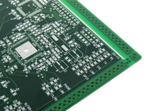
Printed Circuit Boards (PCBs) are the foundation of virtually all modern electronic devices. The conductive traces and pads on the PCB surface enable electrical connections between components. To ensure optimal solderability, protect the copper from oxidation, and enhance the PCB’s appearance and durability, various surface finishes are applied to the exposed copper areas.
Two popular PCB surface finishes are Lead-Free Hot Air Solder Leveling (HASL) and Electroless Nickel Immersion Gold (ENIG). Each has its advantages and disadvantages in terms of cost, process complexity, solderability, shelf life, and suitability for different applications. Choosing the right PCB finish is crucial for the manufacturing process and end product reliability.
In this article, we will take an in-depth look at Lead-Free HASL and ENIG surface finishes. We’ll examine how each process works, compare their key characteristics and performance metrics, and provide guidance on when to use each finish based on the specific requirements of your PCB Design and application.
What is Lead-Free HASL?
Lead-Free Hot Air Solder Leveling (HASL) is a PCB surface finish that involves dipping the board in a molten solder bath and using hot air knives to remove excess solder, leaving behind a thin, leveled layer of solder on the exposed copper areas.
The HASL Process
- PCB is fluxed to remove oxides and promote solder wetting
- Board is dipped in a molten lead-free solder bath (typically tin-silver-copper alloy)
- Hot air knives blow excess solder off the board, leveling the surface
- PCB is cooled and cleaned to remove any flux residues
Advantages of Lead-Free HASL
- Cost-effective and widely available
- Good solderability and wetting properties
- Provides a solderable surface without additional processing
- Suitable for both Through-hole and surface mount components
- Excellent thermal shock resistance
- Reworkable and easy to repair
Disadvantages of Lead-Free HASL
- Uneven surface due to solder pooling and air knife marks
- Not suitable for fine-pitch components due to lack of flatness
- Thickness variations can affect impedance control
- Limited shelf life due to solder oxidation over time
- High processing temperatures can cause thermal stress on the PCB
- Not suitable for gold wire bonding or contact applications

What is ENIG?
Electroless Nickel Immersion Gold (ENIG) is a PCB surface finish that deposits a thin layer of nickel and gold onto the exposed copper surfaces through a chemical process. The nickel layer provides a barrier against copper diffusion, while the gold layer protects the nickel from oxidation and provides a solderable surface.
The ENIG Process
- PCB is cleaned and microetched to remove oxides and roughen the copper surface
- Board is immersed in an electroless nickel plating bath, depositing a thin nickel layer (3-6 µm)
- PCB is rinsed and immersed in an immersion gold bath, depositing a thin gold layer (0.05-0.2 µm) on top of the nickel
- Board is rinsed, dried, and inspected for quality control
Advantages of ENIG
- Flat and uniform surface finish, ideal for fine-pitch components
- Excellent solderability and wetting properties
- Long shelf life due to gold’s resistance to oxidation
- Suitable for gold wire bonding and contact applications
- Good electrical conductivity and corrosion resistance
- Compatible with a wide range of solder alloys and processes
Disadvantages of ENIG
- Higher cost compared to HASL due to the use of gold
- More complex and time-consuming process
- Potential for “black pad” defect due to improper nickel/gold ratio
- Brittle intermetallic compounds can form during soldering, affecting joint reliability
- Not easily reworkable compared to HASL
- May require additional processes for press-fit or insertion mount components

Comparing Lead-Free HASL and ENIG
| Characteristic | Lead-Free HASL | ENIG |
|---|---|---|
| Cost | Low | High |
| Process Complexity | Simple | Complex |
| Surface Flatness | Uneven | Flat and uniform |
| Solderability | Good | Excellent |
| Shelf Life | Limited | Long |
| Fine-Pitch Compatibility | Limited | Excellent |
| Wire Bonding Compatibility | Poor | Good |
| Reworkability | Easy | Difficult |
| Thermal Shock Resistance | Excellent | Good |
| Corrosion Resistance | Good | Excellent |
When to Use Lead-Free HASL
Lead-Free HASL is a suitable choice for PCBs with the following requirements:
– Cost-sensitive applications
– Simple designs with larger component pitches
– Through-hole and surface mount components
– Applications requiring good thermal shock resistance
– Designs that may need rework or repair
– Prototyping and low-volume production
When to Use ENIG
ENIG is the preferred surface finish for PCBs with the following requirements:
– High-density designs with fine-pitch components
– Applications requiring a flat and uniform surface
– Gold wire bonding or contact applications
– Long shelf life and storage requirements
– Designs with strict electrical performance requirements
– High-reliability and mission-critical applications
– High-volume production and automation

ENIG and Lead-Free HASL Processing Considerations
ENIG Processing Considerations
- Proper control of nickel and gold layer thicknesses is crucial for optimal performance
- Nickel/gold ratio must be carefully balanced to avoid “black pad” defect
- Cleanliness and control of the plating baths are essential to ensure a consistent finish
- Proper rinsing and drying between process steps to prevent contamination
- Strict quality control and inspection procedures to detect defects and ensure conformance to specifications
Lead-Free HASL Processing Considerations
- Proper control of solder bath temperature and composition is essential for a consistent finish
- Air knife pressure and angle must be optimized to minimize solder pooling and uneven surfaces
- Flux selection and application are critical for good solderability and preventing defects
- Cooling rate and post-process cleaning must be controlled to minimize thermal stress and residues
- Visual inspection and flatness measurements are necessary to ensure quality and conformance to requirements
Solderability and Reliability Considerations
ENIG Solderability and Reliability
- ENIG provides excellent solderability due to the gold layer’s resistance to oxidation
- Gold layer must be thin enough to prevent embrittlement of solder joints
- Proper nickel layer thickness is crucial for preventing solder joint failure due to intermetallic compound formation
- ENIG is compatible with a wide range of solder alloys and processes, including lead-free and high-temperature soldering
- Gold layer provides good wettability and spreadability of solder, resulting in reliable joints
Lead-Free HASL Solderability and Reliability
- Lead-Free HASL provides good solderability due to the pre-applied solder layer
- Solder bath composition must be carefully controlled to ensure good wetting and spreading properties
- Uneven surface and solder pooling can affect solder joint reliability, particularly for fine-pitch components
- Solder oxidation over time can degrade solderability, limiting the PCB’s shelf life
- Thermal shock resistance is excellent due to the solder layer’s ability to absorb stress
Cost and Availability Considerations
ENIG Cost and Availability
- ENIG is more expensive than Lead-Free HASL due to the use of gold and the more complex process
- Gold price fluctuations can significantly impact the overall cost of ENIG
- ENIG processing requires specialized equipment and trained personnel, which may limit its availability
- Higher cost may be justified for high-reliability and mission-critical applications
Lead-Free HASL Cost and Availability
- Lead-Free HASL is a cost-effective surface finish option, widely available in PCB manufacturing facilities
- Solder bath composition and processing costs are relatively stable and predictable
- Simple process and equipment requirements make Lead-Free HASL a readily accessible option
- Lower cost makes it suitable for prototyping, low-volume production, and cost-sensitive applications
FAQs
1. Can ENIG be used for press-fit or insertion mount components?
ENIG may not be the best choice for press-fit or insertion mount components due to the thin gold layer. The nickel layer can be too hard and brittle, leading to damage during the press-fit process. In these cases, a thicker gold layer (such as Electroless Nickel Electroless Palladium Immersion Gold, ENEPIG) or a different surface finish (such as Immersion Tin) may be more suitable.
2. How does the shelf life of ENIG compare to Lead-Free HASL?
ENIG has a significantly longer shelf life compared to Lead-Free HASL. The gold layer in ENIG protects the underlying nickel from oxidation, preserving solderability for up to 12 months or more. In contrast, the exposed solder surface in Lead-Free HASL can oxidize over time, degrading solderability and limiting the shelf life to 3-6 months, depending on storage conditions.
3. Can Lead-Free HASL be used for gold wire bonding applications?
No, Lead-Free HASL is not suitable for gold wire bonding applications. The uneven solder surface and the presence of the solder layer itself are incompatible with the wire bonding process. ENIG, with its flat gold surface, is a better choice for gold wire bonding applications.
4. What is the “black pad” defect in ENIG, and how can it be prevented?
The “black pad” defect in ENIG occurs when an excessive amount of the underlying nickel layer is corroded during the immersion gold process. This results in a thin, weak, or non-existent nickel layer beneath the gold, leading to poor solderability and potential joint failure. To prevent this defect, the nickel and gold layer thicknesses must be carefully controlled, and the plating baths must be properly maintained and monitored.
5. Can Lead-Free HASL be used for high-frequency or RF applications?
Lead-Free HASL may not be the best choice for high-frequency or RF applications due to its uneven surface and potential for solder pooling, which can affect impedance control and signal integrity. ENIG, with its flat and uniform surface, is generally a better option for these applications. However, the specific requirements of the design and the performance trade-offs should be carefully evaluated when selecting a surface finish for high-frequency or RF PCBs.
Conclusion
Lead-Free HASL and ENIG are two popular PCB surface finishes, each with its own advantages and disadvantages. Lead-Free HASL offers a cost-effective solution with good solderability, thermal shock resistance, and reworkability, making it suitable for simple designs, prototyping, and low-volume production. ENIG, on the other hand, provides a flat and uniform surface, excellent solderability, long shelf life, and compatibility with fine-pitch components and gold wire bonding, making it ideal for high-density designs, high-reliability applications, and high-volume production.
When selecting between Lead-Free HASL and ENIG, it is essential to consider the specific requirements of your PCB design and application, including cost, performance, reliability, and manufacturing constraints. By understanding the characteristics, processing considerations, and trade-offs of each surface finish, you can make an informed decision that balances your technical and economic needs.
As PCB technology continues to evolve, new surface finish options may emerge to address the ever-increasing demands of advanced electronic applications. However, Lead-Free HASL and ENIG remain two of the most widely used and proven surface finishes in the industry today, offering a range of benefits for a wide variety of PCB designs and applications.


Leave a Reply