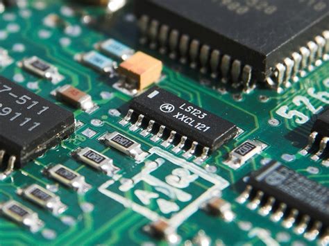
Understanding the Basics of PCB Design
Before diving into the tips and tricks, it’s essential to understand the basics of PCB design. A PCB is a board made of insulating materials, such as fiberglass or plastic, with conductive copper traces printed on its surface. These traces connect various electronic components, such as resistors, capacitors, and integrated circuits (ICs), to form a complete circuit.
PCBs come in different types, depending on the number of layers and the placement of components. The most common types are:
- Single-Sided PCBs: These have components and traces on only one side of the board.
- Double-sided PCBs: These have components and traces on both sides of the board.
- Multi-layer PCBs: These have more than two layers, with traces running between the layers.
When designing a PCB, it’s crucial to consider factors such as the size of the board, the number of layers, the placement of components, and the routing of traces. These factors can affect the performance, reliability, and cost of the final product.
Tip 1: Choose the Right Software
Choosing the right PCB design software is the first step towards creating a successful PCB. There are many software options available, ranging from free open-source tools to expensive commercial packages. Some popular PCB design software include:
- KiCad: A free and open-source PCB design tool that supports schematic capture, PCB Layout, and 3D viewing.
- Eagle: A popular commercial PCB design tool that offers a wide range of features and libraries.
- Altium Designer: A high-end PCB design tool that provides advanced features such as simulation and analysis.
When choosing a PCB design software, consider factors such as ease of use, availability of libraries and components, and compatibility with other tools and formats. It’s also important to consider the cost and licensing options, especially if you’re working on a budget.

Tip 2: Plan Your Design
Before starting the actual design process, it’s essential to plan your PCB layout. This involves creating a schematic diagram that shows the connections between the various components. A schematic diagram is a graphical representation of the circuit, with symbols representing the components and lines representing the connections.
When creating a schematic diagram, follow these best practices:
- Use standard symbols for components, such as resistors, capacitors, and ICs.
- Label all components with their values and part numbers.
- Use net labels to identify the connections between components.
- Group related components together to make the schematic easier to read.
Once you have a schematic diagram, you can start planning the physical layout of the PCB. This involves deciding on the size and shape of the board, the placement of components, and the routing of traces.

Tip 3: Consider the Board Size and Shape
The size and shape of the PCB can have a significant impact on its performance and cost. When designing a PCB, consider the following factors:
- The available space in the final product: The PCB must fit inside the enclosure or housing of the final product, so it’s essential to consider the available space when deciding on the size and shape of the board.
- The number and size of components: The size and number of components on the board will determine the minimum size of the PCB. It’s important to leave enough space between components to avoid interference and overheating.
- The manufacturing process: The size and shape of the PCB can affect the manufacturing process and cost. For example, smaller boards may require more precise manufacturing techniques, which can increase the cost.
When deciding on the size and shape of the PCB, it’s also important to consider the placement of connectors and mounting holes. Connectors should be placed near the edge of the board for easy access, while mounting holes should be placed in a way that ensures the board is securely fastened to the enclosure.

Tip 4: Choose the Right Components
Choosing the right components is crucial for the performance and reliability of the PCB. When selecting components, consider the following factors:
- Functionality: The components must perform the desired function in the circuit. For example, if you need a Voltage Regulator, choose a component that can handle the required voltage and current.
- Availability: The components must be readily available from suppliers. It’s important to choose components that are not obsolete or hard to find.
- Cost: The cost of the components can have a significant impact on the overall cost of the PCB. It’s important to choose components that provide the required functionality at a reasonable cost.
- Footprint: The footprint of the component must match the footprint on the PCB. It’s important to choose components with standard footprints to avoid compatibility issues.
When choosing components, it’s also important to consider their thermal characteristics. Components that generate a lot of heat, such as power transistors and voltage regulators, may require additional cooling measures, such as heatsinks or fans.
Tip 5: Route the Traces Carefully
Routing the traces on the PCB is one of the most critical aspects of PCB design. The traces carry the electrical signals between the components, so it’s essential to route them carefully to avoid signal integrity issues and electromagnetic interference (EMI).
When routing traces, follow these best practices:
- Keep the traces as short as possible to minimize signal loss and delay.
- Avoid sharp angles and corners, which can cause signal reflections and EMI.
- Use a consistent trace width throughout the board to maintain signal integrity.
- Separate sensitive traces, such as clock and data lines, from noisy traces, such as power and ground.
- Use ground planes to provide a low-impedance return path for the signals.
It’s also important to consider the current-carrying capacity of the traces. The width of the trace must be sufficient to carry the required current without overheating or causing voltage drops.
Tip 6: Use Proper Grounding Techniques
Proper grounding is essential for the performance and reliability of the PCB. Ground planes provide a low-impedance return path for the signals and help to reduce EMI.
When designing the ground planes, follow these best practices:
- Use a solid ground plane on one or more layers of the PCB.
- Connect all ground pins of the components to the ground plane using vias.
- Use multiple vias for high-current components to reduce the impedance of the ground connection.
- Avoid splitting the ground plane, which can cause ground loops and EMI.
It’s also important to consider the placement of the ground vias. The vias should be placed as close as possible to the ground pins of the components to minimize the loop area and reduce EMI.
Tip 7: Consider the Manufacturing Process
The manufacturing process can have a significant impact on the cost and reliability of the PCB. When designing the PCB, consider the following factors:
- The number of layers: The number of layers in the PCB can affect the manufacturing cost and complexity. It’s important to choose the minimum number of layers that provide the required functionality and performance.
- The type of vias: There are different types of vias, such as through-hole, blind, and buried vias. The type of via can affect the manufacturing cost and complexity, so it’s important to choose the appropriate type for the design.
- The minimum trace width and spacing: The minimum trace width and spacing can affect the manufacturing cost and yield. It’s important to choose values that are within the capabilities of the manufacturing process.
- The type of finish: The type of finish on the PCB, such as HASL or ENIG, can affect the cost and reliability of the board. It’s important to choose a finish that provides the required protection and solderability.
When designing the PCB, it’s also important to communicate with the manufacturer to ensure that the design is compatible with their process and capabilities.
Tip 8: Test and Verify the Design
Testing and verifying the PCB design is an essential step in the design process. It helps to identify and correct any issues before the board is manufactured, which can save time and cost in the long run.
When testing the PCB design, follow these best practices:
- Use simulation tools to verify the functionality and performance of the circuit.
- Use design rule checks (DRC) to verify that the design meets the manufacturing requirements and constraints.
- Use electrical rule checks (ERC) to verify that the design meets the electrical requirements and constraints.
- Use 3D viewing tools to verify the mechanical fit and clearance of the components.
It’s also important to perform physical testing of the manufactured board to ensure that it meets the required functionality and performance.
Tip 9: Document the Design
Documenting the PCB design is an essential step in the design process. It helps to communicate the design intent and requirements to the manufacturing team and other stakeholders.
When documenting the PCB design, include the following information:
- The schematic diagram, showing the connections between the components.
- The Bill of Materials (BOM), listing all the components used in the design.
- The PCB layout, showing the placement and routing of the components and traces.
- The assembly drawing, showing the placement and orientation of the components on the board.
- The fabrication drawing, showing the dimensions and specifications of the board.
It’s also important to include any special instructions or requirements, such as the type of finish or the required testing procedures.
Tip 10: Keep Learning and Improving
PCB design is a constantly evolving field, with new technologies and techniques emerging all the time. To stay competitive and produce high-quality designs, it’s essential to keep learning and improving your skills.
Some ways to keep learning and improving include:
- Attending training courses and workshops on PCB design and related topics.
- Reading industry publications and blogs to stay up-to-date on the latest trends and best practices.
- Participating in online forums and communities to share knowledge and learn from others.
- Experimenting with new tools and techniques to improve your design process and outcomes.
By continuously learning and improving, you can stay ahead of the curve and produce PCBs that meet the highest standards of quality and performance.
FAQ
-
What is the best software for PCB design?
There is no one “best” software for PCB design, as different tools have different strengths and weaknesses. Some popular options include KiCad, Eagle, and Altium Designer. The best software for you will depend on your specific needs, budget, and level of expertise. -
How do I choose the right components for my PCB?
When choosing components for your PCB, consider factors such as functionality, availability, cost, and footprint. Choose components that provide the required functionality at a reasonable cost, and ensure that they are readily available from suppliers. Also, make sure that the footprint of the component matches the footprint on the PCB. -
What is the importance of proper grounding in PCB design?
Proper grounding is essential for the performance and reliability of the PCB. Ground planes provide a low-impedance return path for the signals and help to reduce electromagnetic interference (EMI). When designing the ground planes, use a solid ground plane on one or more layers of the PCB, and connect all ground pins of the components to the ground plane using vias. -
How can I ensure that my PCB design is manufacturable?
To ensure that your PCB design is manufacturable, consider factors such as the number of layers, the type of vias, the minimum trace width and spacing, and the type of finish. Choose values that are within the capabilities of the manufacturing process, and communicate with the manufacturer to ensure that the design is compatible with their process and capabilities. -
What are some ways to keep learning and improving my PCB design skills?
To keep learning and improving your PCB design skills, attend training courses and workshops, read industry publications and blogs, participate in online forums and communities, and experiment with new tools and techniques. By continuously learning and improving, you can stay ahead of the curve and produce high-quality PCB designs.
| Factor | Consideration |
|---|---|
| Board Size and Shape | – Available space in the final product – Number and size of components – Manufacturing process and cost |
| Component Selection | – Functionality – Availability – Cost – Footprint |
| Trace Routing | – Keep traces short – Avoid sharp angles and corners – Use consistent trace width – Separate sensitive traces from noisy traces – Use ground planes |
| Grounding Techniques | – Use solid ground plane – Connect all ground pins to ground plane using vias – Use multiple vias for high-current components – Avoid splitting the ground plane |
| Manufacturing Process | – Number of layers – Type of vias – Minimum trace width and spacing – Type of finish |
In conclusion, designing a reliable and efficient PCB requires careful consideration of various factors, from choosing the right software and components to routing traces and documenting the design. By following the tips and tricks outlined in this article, you can create PCBs that meet the highest standards of quality and performance. Remember to keep learning and improving your skills, and don’t hesitate to seek help and advice from the PCB design community when needed.


Leave a Reply