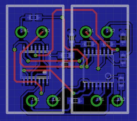
What is PCB Layout?
PCB layout, also known as printed circuit board layout, is the process of designing the physical layout of a printed circuit board (PCB). It involves arranging components and routing traces on a PCB to create a functional electronic circuit. The layout process is critical in ensuring that the PCB meets the required specifications, performs reliably, and is cost-effective to manufacture.
Key Elements of PCB Layout
- Component Placement
- Trace Routing
- Power and Ground Planes
- Signal Integrity
- Manufacturability
Why is PCB Layout Important?
A well-designed PCB layout is essential for several reasons:
-
Functionality: A proper layout ensures that the electronic circuit functions as intended, with minimal interference and signal integrity issues.
-
Reliability: A good layout minimizes the risk of failures caused by manufacturing defects, environmental factors, or component stress.
-
Cost-effectiveness: An optimized layout reduces manufacturing costs by minimizing the board size, layer count, and component count.
-
Electromagnetic Compatibility (EMC): A well-designed layout minimizes electromagnetic interference (EMI) and ensures compliance with EMC regulations.

PCB Layout Design Process
The PCB layout design process typically involves the following steps:
-
Schematic Review: The layout designer reviews the electronic schematic to understand the circuit requirements and identifies any potential issues.
-
Component Placement: The designer places components on the board, considering factors such as signal flow, heat dissipation, and mechanical constraints.
-
Trace Routing: The designer routes traces between components, ensuring that signal integrity, EMC, and manufacturability requirements are met.
-
Power and Ground Planes: The designer creates power and ground planes to provide a stable reference voltage and minimize noise.
-
Design Rule Check (DRC): The designer runs a DRC to ensure that the layout meets the manufacturing and electrical constraints.
-
Output Generation: The designer generates output files, such as Gerber files, drill files, and assembly drawings, for manufacturing.

PCB Layout Design Guidelines
To create a successful PCB layout, designers should follow these guidelines:
-
Keep traces as short as possible: Shorter traces minimize signal delay, attenuation, and crosstalk.
-
Avoid sharp angles: Use 45-degree angles or curved traces to minimize reflections and signal integrity issues.
-
Provide adequate clearance: Ensure sufficient clearance between components, traces, and board edges to avoid short circuits and manufacturing issues.
-
Use appropriate trace widths: Select trace widths based on the current carrying capacity and signal integrity requirements.
-
Minimize crosstalk: Separate sensitive signals from noisy signals, and use ground planes and shielding to minimize crosstalk.
-
Consider thermal management: Place heat-generating components away from sensitive components, and provide adequate cooling and heat sinking.
-
Follow manufacturability guidelines: Adhere to the manufacturer’s design rules and guidelines to ensure that the board can be reliably manufactured.

PCB Layout Software
There are several software tools available for PCB layout design, including:
- Altium Designer
- Cadence Allegro
- Mentor Graphics PADS
- KiCad
- Eagle
These tools provide a range of features and capabilities, from simple schematic capture and layout to advanced signal integrity analysis and 3D modeling.
PCB Layout Design Services
Many companies offer PCB layout design services to help customers create high-quality, reliable PCBs. These services typically include:
-
Schematic Review: The service provider reviews the customer’s schematic and provides feedback on potential issues and improvements.
-
Component Selection: The service provider helps the customer select appropriate components based on the circuit requirements and availability.
-
PCB Layout: The service provider creates the PCB layout based on the customer’s requirements and design guidelines.
-
Design Review: The service provider reviews the layout with the customer and incorporates any feedback or changes.
-
Output Generation: The service provider generates the necessary output files for manufacturing.
| Service | Description |
|---|---|
| Schematic Review | Review customer’s schematic and provide feedback |
| Component Selection | Help customer select appropriate components |
| PCB Layout | Create PCB layout based on customer’s requirements |
| Design Review | Review layout with customer and incorporate feedback |
| Output Generation | Generate necessary output files for manufacturing |
Benefits of Using a PCB Layout Design Service
Using a PCB layout design service offers several benefits:
-
Expertise: Service providers have experienced designers who can create high-quality layouts that meet the customer’s requirements.
-
Time Savings: Outsourcing the layout design process allows customers to focus on their core competencies and reduces time-to-market.
-
Cost Savings: Service providers can often create layouts more efficiently and cost-effectively than in-house teams, especially for complex designs.
-
Quality Assurance: Service providers use established design processes and quality control measures to ensure that the layout meets the required specifications.
Choosing a PCB Layout Design Service
When choosing a PCB layout design service, consider the following factors:
-
Experience: Look for a service provider with experience in designing PCBs similar to your requirements.
-
Capabilities: Ensure that the service provider has the necessary software tools and expertise to handle your design complexity.
-
Communication: Choose a service provider that communicates effectively and responds promptly to your queries and feedback.
-
Cost: Compare the costs of different service providers, but don’t compromise on quality for the sake of lower costs.
-
Turnaround Time: Consider the service provider’s turnaround time and ensure that it meets your project timeline.
Conclusion
PCB layout design is a critical step in the development of electronic products. A well-designed layout ensures that the PCB functions reliably, meets the required specifications, and is cost-effective to manufacture. Using a PCB layout design service can help customers create high-quality layouts efficiently and cost-effectively, while allowing them to focus on their core competencies.
Frequently Asked Questions (FAQ)
-
What is the difference between PCB layout and PCB design?
PCB design encompasses the entire process of creating a PCB, including schematic capture, component selection, and layout. PCB layout specifically refers to the process of arranging components and routing traces on the board. -
How long does it take to create a PCB layout?
The time required to create a PCB layout depends on the complexity of the design and the experience of the designer. Simple layouts can be completed in a few hours, while complex layouts can take several weeks. -
What are the most common PCB layout mistakes?
Common PCB layout mistakes include inadequate clearance between components and traces, incorrect trace widths, poor signal integrity, and failure to follow manufacturability guidelines. -
Can I use autorouting for PCB layout?
Autorouting can be used for simple PCB layouts, but it is not recommended for complex designs. Manual routing by an experienced designer is often necessary to ensure optimal signal integrity and manufacturability. -
What files do I need to provide to a PCB layout design service?
To use a PCB layout design service, you typically need to provide a schematic, bill of materials (BOM), and any specific design requirements or constraints. The service provider may also request additional information, such as component datasheets and mechanical drawings.


Leave a Reply