Introduction to Printed Circuit Boards
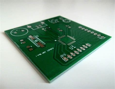
Printed Circuit Boards (PCBs) are the backbone of modern electronics. They are used in almost every electronic device, from smartphones and laptops to medical equipment and aerospace systems. PCBs are designed to mechanically support and electrically connect electronic components using conductive pathways, tracks, or signal traces etched from copper sheets laminated onto a non-conductive substrate.
Types of Printed Circuit Boards
There are several types of PCBs, each with its own unique characteristics and applications:
- Single-Sided PCBs: These have conductive traces on only one side of the substrate.
- Double-sided PCBs: These have conductive traces on both sides of the substrate.
- Multi-layer PCBs: These consist of multiple layers of conductive traces separated by insulating layers.
- Flexible PCBs: These are made from flexible materials, allowing them to bend and conform to different shapes.
- Rigid-flex PCBs: These combine rigid and flexible sections, offering the benefits of both types.
Factors Affecting the Mass of Printed Circuit Boards
The mass of a PCB depends on several factors, including:
PCB Dimensions
The length, width, and thickness of a PCB directly impact its mass. Larger PCBs with more layers will have a greater mass compared to smaller, single-layer boards.
PCB Materials
The materials used in the construction of a PCB also affect its mass. The most common materials include:
- FR-4: A composite material made from woven fiberglass cloth with an epoxy resin binder. It is the most widely used PCB substrate material.
- Aluminum: Used for PCBs that require better thermal management or mechanical stability.
- Polyimide: A flexible polymer used for flexible PCBs.
- Copper: Used for the conductive traces on the PCB. The thickness of the copper layer can vary, impacting the overall mass of the board.
Component Density
The number and type of components mounted on a PCB also contribute to its mass. Boards with a higher component density will generally have a greater mass than those with fewer components.

Calculating the Mass of a Printed Circuit Board
To calculate the mass of a PCB, you need to know its dimensions, the density of the materials used, and the volume of any additional components. The general formula for calculating the mass of a rectangular PCB is:
Mass = Length × Width × Thickness × Density
For example, consider an FR-4 PCB with the following dimensions:
- Length: 100 mm
- Width: 80 mm
- Thickness: 1.6 mm
- Density of FR-4: 1.85 g/cm³
The mass of the PCB can be calculated as follows:
Mass = 100 mm × 80 mm × 1.6 mm × 1.85 g/cm³
     = 23.68 g
To this value, you would need to add the mass of any components mounted on the board to determine the total mass of the assembled PCB.

PCB Mass and Manufacturing Considerations
The mass of a PCB can have implications for the manufacturing process and the final application of the assembled board.
Manufacturing Process
In the PCB manufacturing process, the mass of the board can affect:
- Handling: Heavier boards may require specialized handling equipment and may be more prone to damage during transport.
- Etching: The time required for etching the conductive traces may vary depending on the thickness and density of the copper layer.
- Drilling: The mass of the board can impact the wear on drilling equipment and the time required for drilling operations.
Final Application
The mass of an assembled PCB can also have implications for its final application, such as:
- Mechanical stress: Heavier boards may be more susceptible to mechanical stress, particularly in applications with high levels of vibration or shock.
- Thermal management: The mass of a PCB can affect its thermal characteristics, influencing heat dissipation and the need for additional cooling measures.
- Weight restrictions: In certain applications, such as aerospace or portable devices, the mass of the PCB may be a critical factor due to weight restrictions.

Optimizing PCB Mass
In some cases, it may be necessary to optimize the mass of a PCB to meet specific application requirements or to reduce manufacturing costs. Some strategies for optimizing PCB mass include:
Material Selection
Choosing lighter materials, such as high-performance polymers or composite substrates, can help reduce the overall mass of the PCB without compromising its electrical or mechanical properties.
Miniaturization
Reducing the size of the PCB and its components can significantly decrease its mass. This can be achieved through the use of smaller components, higher-density layouts, and advanced packaging techniques.
Hollowing Techniques
For applications where mass reduction is critical, techniques such as backdropping or pocket milling can be used to selectively remove material from the PCB substrate, creating hollow areas that reduce the overall mass of the board.
Component Placement Optimization
Strategically placing components on the PCB can help balance the mass distribution and minimize the need for additional mechanical support structures.
FAQ
- What is the most common material used for PCB substrates?
-
FR-4, a composite material made from woven fiberglass cloth with an epoxy resin binder, is the most widely used PCB substrate material.
-
How does the thickness of the copper layer affect the mass of a PCB?
-
The thickness of the copper layer directly impacts the mass of the PCB. Thicker copper layers will result in a heavier board, while thinner layers will produce a lighter board.
-
What is backdropping in PCB manufacturing?
-
Backdropping is a technique used to selectively remove material from the PCB substrate, creating hollow areas that reduce the overall mass of the board. This is particularly useful in applications where mass reduction is critical.
-
How can miniaturization help reduce the mass of a PCB?
-
Miniaturization involves reducing the size of the PCB and its components, which can significantly decrease the overall mass of the board. This can be achieved through the use of smaller components, higher-density layouts, and advanced packaging techniques.
-
Why is the mass of a PCB important in aerospace applications?
- In aerospace applications, the mass of a PCB is critical due to weight restrictions. Lighter PCBs can help reduce the overall weight of the aircraft, improving fuel efficiency and performance.
Conclusion
Printed Circuit Boards are essential components in modern electronics, and their mass plays a crucial role in both the manufacturing process and the final application. The mass of a PCB is influenced by factors such as its dimensions, materials, and component density. Calculating the mass of a PCB involves considering these factors and using the appropriate formula.
Optimizing the mass of a PCB may be necessary to meet specific application requirements or to reduce manufacturing costs. Strategies for mass optimization include material selection, miniaturization, hollowing techniques, and component placement optimization.
Understanding the factors that affect PCB mass and the strategies for optimizing it is essential for engineers, designers, and manufacturers working with Printed Circuit Boards. By considering the mass of a PCB throughout the design and manufacturing process, it is possible to create more efficient, reliable, and cost-effective electronic devices.
| PCB Type | Typical Thickness Range (mm) | Common Applications |
|---|---|---|
| Single-sided | 0.8 – 1.6 | Simple electronic circuits, low-cost devices |
| Double-sided | 0.8 – 2.4 | More complex circuits, higher component density |
| Multi-layer | 0.8 – 3.2 | High-density circuits, advanced electronic devices |
| Flexible | 0.05 – 0.25 | Wearable electronics, compact devices |
| Rigid-Flex | Varies based on design | Complex devices requiring both rigid and flexible sections |


Leave a Reply