Introduction to PCB Copper Trace Width and Current
Printed circuit boards (PCBs) are the foundation of nearly all modern electronics. Proper PCB design is critical to ensure reliable operation, signal integrity, power delivery, and heat dissipation. One of the most important aspects of PCB design is selecting the appropriate width of the copper traces for the amount of current they need to carry.
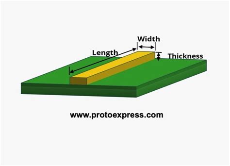
The width of a PCB trace determines its cross-sectional area, which in turn determines its resistance and current carrying capacity. Wider traces have lower resistance and can handle higher currents without excessive heating. Narrower traces have higher resistance and are limited to lower current levels to prevent damage.
In this article, we’ll dive deep into the relationship between PCB copper trace width, thickness, and current carrying capacity. We’ll look at how to calculate the maximum current for a given trace width, how to size traces for your design requirements, and best practices for High-current PCB design. Whether you’re a PCB designer, electrical engineer, or electronics enthusiast, understanding this critical aspect of PCB layout is essential for creating robust and reliable designs.
Factors That Affect PCB Trace Current Capacity
Several key factors influence the current carrying capacity of a PCB trace:
Trace Width
The wider a trace is, the more current it can handle. Doubling the width of a trace halves its resistance and allows it to carry twice as much current for a given temperature rise.
Copper Thickness
PCBs use copper foil laminated onto an insulating substrate. The thickness of this copper layer, measured in ounces per square foot, also affects current capacity. Thicker copper allows higher currents. Standard PCB Copper Weights are 1 oz (35 μm thick) and 2 oz (70 μm).
Allowable Temperature Rise
Current flow through a trace causes heating due to the resistance of the copper. The more heating that is allowed, the more current a trace can handle. Typical PCB designs permit a 10°C temperature rise in traces.
Ambient Temperature
The temperature of the environment around a PCB factors into how much current its traces can carry. Higher ambient temperatures mean traces can handle less current before overheating.
Trace Length
Longer traces have more resistance than shorter traces of the same width and thickness. A very long trace may need to be wider to accommodate the same current as a shorter trace.

How to Calculate PCB Trace Current Capacity
To determine how much current a PCB trace can safely carry, we need to know its cross-sectional area and the allowable temperature rise. There are several ways to approach this calculation.
PCB Trace Current Capacity Tables
Many PCB design guides include lookup tables that provide the current capacity for common trace widths and copper thicknesses at a specified temperature rise:
| Trace Width (mils) | 1 oz Cu Current (A) | 2 oz Cu Current (A) |
|---|---|---|
| 10 | 0.5 | 0.7 |
| 20 | 1.0 | 1.4 |
| 30 | 1.5 | 2.1 |
| 50 | 2.5 | 3.5 |
| 100 | 4.9 | 6.9 |
Currents are for outer layer traces on 1.6 mm FR-4 PCBs with 10°C rise in still air at 25°C ambient.
These tables provide a quick reference but are limited to specific conditions. For other scenarios, we need to use formulas that factor in trace geometry and environment.
IPC-2221 Formulas for Internal and External PCB Trace Currents
The IPC-2221 generic standard on PCB design provides guidelines and formulas for calculating trace currents under various conditions.
For traces on outer layers with 10°C rise above ambient:
I = 0.065 * dT^0.44 * A^0.725
And for traces on inner layers or with 20°C rise:
I = 0.041 * dT^0.45 * A^0.680
Where:
– I = maximum current in amps
– dT = temperature rise above ambient in °C
– A = cross-sectional area of trace in mils^2 (1 mil = 0.001 inch)
The cross-sectional area A is simply the trace width in mils times the copper thickness in mils (1 oz Cu is 1.4 mils thick, 2 oz is 2.8 mils thick).
For example, a 100 mil wide, 1 oz trace on an outer layer with 10°C rise:
A = 100 * 1.4 = 140 mils^2
I = 0.065 * 10^0.44 * 140^0.725 = 4.9 A
Which matches the value from the earlier table. You can use these formulas to calculate the current capacity for any trace geometry and environment.
Online PCB Trace Current Calculators
For quick results, there are many online calculators that implement the IPC-2221 formulas. Simply enter the trace width, copper thickness, layer, and temperature rise and the calculator provides the maximum current.
Some advanced calculators add extra parameters like trace length, ambient temperature, and conductor material to further refine the results. These tools are very handy for PCB designers.

Sizing PCB Traces for Current Capacity
When laying out a PCB, an important step is to determine the minimum trace widths needed for each signal based on its expected maximum current. There are a few ways to approach trace width sizing.
Rule of Thumb for Trace Width vs. Current
A quick rule of thumb is to allow 10 mils of trace width for every 1 A of current on an outer layer (half that for inner layers). This is a conservative guideline that works for most common situations with 10°C rise and 1 oz copper.
For example, a trace carrying 2 A should be at least 20 mils wide on an outer layer, or 40 mils wide on an inner layer. Note that this is just a starting point – the actual minimum width should be calculated based on the specific PCB Stackup and environment.
Solving PCB Trace Current Formulas for Width
The IPC-2221 trace current formulas can be solved for width if the maximum current is known. Assuming 1 oz copper:
A = (I / (0.065 * dT^0.44))^(1/0.725)
width = A / 1.4
Plugging in I=2 A and dT=10°C:
A = (2 / (0.065 * 10^0.44))^(1/0.725) = 61 mils^2
width = 61 / 1.4 = 44 mils
So for 2 A with a 10°C rise, a 1 oz trace should be at least 44 mils wide. Bumping up to the next standard trace size of 50 mils is a good idea. Again, an online calculator makes this math easy.
Simulating Trace Heating in PCB Design Tools
Modern PCB design software often includes thermal simulation tools that can analyze your PCB layout and identify traces that may overheat based on their width, current, and environment.
These tools factor in many aspects like copper thickness, air flow, board cooling, thermal reliefs, and the heating of nearby components and traces. They provide a color-coded view of predicted trace and board temperatures.
Running a thermal simulation is a good way to double-check that your trace widths are sufficient for your design prior to manufacturing. It can help you spot problem areas and optimize the routing for better current handling and heat dissipation.

Best Practices for High Current PCB Design
Designing boards to carry high currents for power electronics requires extra care to ensure reliable operation and long service life. Here are some tips for high-current PCB design:
Use Wide Traces and Planes Where Possible
Traces carrying more than a few amps should be very wide to minimize resistance and heating. If a trace is carrying more than 5-10 A, consider using a copper pour or plane instead. Wider traces and larger copper areas also help with heat dissipation.
Use Thicker Copper for High Current Traces
Choosing 2 oz or even 3 oz copper for inner and outer layers provides significantly more current capacity than standard 1 oz copper. The added cost of thicker copper is usually well worth it for high-power designs.
Minimize High Current Trace Lengths
Keeping high-current traces as short as possible reduces resistance and power losses. Place high-current components close together and use direct routes for their interconnects.
Use Thermal Reliefs and Vias
Soldering components to large copper areas can be difficult due to the heat sinking effect. Adding thermal reliefs (aka thermals or spokes) to component pads on planes eases soldering while maintaining current capacity.
High current vias should be larger than signal vias to lower resistance. Multiple vias in parallel can share the current load. Vias also transfer heat to inner planes for better cooling.
Allow for Adequate Trace Spacing
High currents can cause significant magnetic fields around traces which may induce crosstalk on nearby signal traces. Provide extra spacing between high current and low current traces. Also leave space for heat dissipation.
Provide Solid Grounding and Power Planes
Trying to route high currents through thin ground traces is asking for trouble. Use ground planes and power planes to provide low-impedance current return paths. Consider multi-layer boards for better power distribution.
Use Copper Pours for Heatsinking
Large copper pours on outer layers connected to ground or power planes help spread and dissipate the heat generated by high current traces and components. This is especially important for surface mount power components with exposed pads.
Consider Paralleling Traces or Layers
For very high currents, running multiple traces or even dedicated layers in parallel can share the current and reduce the width required for each individual trace or layer. Just be sure to break up parallel paths to avoid creating unintended coils.
FAQ on PCB Trace Current and Width
What happens if a PCB trace is too narrow for the current it carries?
If a trace is too thin for the current flowing through it, several bad things can happen:
– The trace will heat up due to its resistance, possibly to the point of melting or burning up, causing board failure
– The trace may become a fuse and burn out, creating an open circuit
– Excessive heating may damage nearby components or the PCB substrate material
– Circuit performance may suffer due to the high resistance and voltage drop across the undersized trace
How much current can a 10 mil trace handle?
It depends on several factors, but for a typical 1 oz copper outer layer trace on an FR-4 PCB with a 10°C temperature rise, a 10 mil trace can handle about 0.5 A continuously. Bumping up to 2 oz copper increases that to about 0.7 A.
What’s a good minimum trace width for power traces?
A good rule of thumb is to use at least 50 mil traces for power connections and traces carrying more than a few amps. This provides a good balance of current capacity and routability for most designs. Of course, the actual width needed should be calculated based on the expected current and allowable temperature rise.
What is the maximum current carrying capacity of a PCB trace?
There is no hard upper limit to how much current a PCB trace can handle – it depends on its width, thickness, length, and allowable temperature rise. In practice, currents above 10-20 A are usually carried by very wide traces or copper pours and planes spanning large areas of the board.
How do you size PCB traces for high current?
The key steps for sizing high-current PCB traces are:
1. Determine the maximum expected current for each high-power net
2. Decide on an appropriate temperature rise, copper thickness, and trace length
3. Use the IPC-2221 formulas, manufacturer charts, or online calculators to find the minimum trace width needed for each current level
4. Round up to the next larger standard trace width for each high current net, leaving some margin
5. Run a thermal simulation on the PCB layout to check for any potential hot spots or overloaded traces
6. Modify trace widths and layouts as needed to stay within acceptable temperature and voltage drop limits
Careful planning, calculations, and thermal analysis are important to ensure reliable high-current operation.
Conclusion
The width and thickness of PCB traces is a critical design factor that determines how much current they can safely carry. Undersized traces can overheat and fail while oversized traces waste space and add cost.
By understanding the key parameters and using the IPC-2221 formulas and charts, it’s straightforward to calculate the appropriate trace widths for a given design. Following best practices like using wide, short traces, thick copper, thermal reliefs, and solid power and ground planes maximizes current capacity.
Simulating designs prior to fabrication and leaving reasonable margins helps ensure that PCBs will perform well under worst-case conditions. Taking the time to properly design and route high-current PCB traces is essential for creating reliable, efficient, and cost-effective boards.


Leave a Reply