Introduction to PCB Stackup
Printed Circuit Board (PCB) stackup refers to the arrangement of copper layers and insulating materials that make up a PCB. Proper PCB stackup planning is crucial for ensuring the optimal performance, reliability, and manufacturability of electronic devices. In this comprehensive guide, we will delve into the intricacies of PCB stackup planning, covering key concepts, best practices, and frequently asked questions.
The Importance of PCB Stackup Planning
Signal Integrity
One of the primary reasons for careful PCB stackup planning is to maintain signal integrity. The arrangement of layers, the choice of materials, and the spacing between layers can significantly impact the quality of signals transmitted through the PCB. Proper stackup design helps minimize signal distortion, crosstalk, and electromagnetic interference (EMI).
Power Integrity
PCB stackup planning also plays a vital role in ensuring power integrity. The placement of power and ground layers, as well as their thickness and spacing, affects the distribution of power throughout the PCB. Optimizing the stackup can help reduce voltage drop, minimize power supply noise, and improve overall power delivery.
Thermal Management
Effective thermal management is another important consideration in PCB stackup planning. The choice of materials, the thickness of layers, and the placement of components can all impact the PCB’s ability to dissipate heat. Proper stackup design helps prevent overheating, which can lead to component failure and reduced reliability.
Manufacturing Feasibility
PCB stackup planning must also take into account manufacturing feasibility. The choice of materials, layer counts, and spacing should align with the capabilities of the PCB manufacturing process. Proper stackup design ensures that the PCB can be manufactured reliably and cost-effectively.

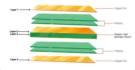
PCB Stackup Layers
A typical PCB stackup consists of multiple layers, each serving a specific purpose. Let’s explore the common layers found in a PCB stackup.
Signal Layers
Signal layers are used for routing electrical signals between components on the PCB. These layers are typically made of copper and are etched with the desired signal traces. The number of signal layers required depends on the complexity of the circuit and the routing requirements.
Power and Ground Planes
Power and ground planes are dedicated layers that provide a low-impedance path for power distribution and grounding. These layers are usually solid copper planes that span the entire PCB. The placement and spacing of power and ground planes are critical for maintaining power integrity and reducing noise.
Dielectric Layers
Dielectric layers, also known as insulating layers, are used to separate and insulate the conductive layers in a PCB stackup. These layers are typically made of materials such as FR-4, Rogers, or other high-performance dielectrics. The choice of dielectric material depends on the desired electrical properties, such as dielectric constant and loss tangent.
Solder Mask and Silkscreen Layers
Solder mask and silkscreen layers are non-conductive layers applied to the outer surfaces of the PCB. The solder mask layer provides insulation and protection for the exposed copper traces, while the silkscreen layer is used for component labeling and identification.

PCB Stackup Configurations
There are various PCB stackup configurations that can be used depending on the specific requirements of the design. Let’s explore some common stackup configurations.
2-Layer Stackup
A 2-Layer PCB stackup is the simplest configuration, consisting of a single signal layer on each side of the dielectric layer. This stackup is suitable for simple, low-density designs with minimal routing requirements.
4-Layer Stackup
A 4-layer PCB stackup is a common configuration for more complex designs. It typically consists of two signal layers, one power plane, and one ground plane. The signal layers are placed on the outer surfaces, while the power and ground planes are sandwiched between the dielectric layers.
6-Layer Stackup
A 6-Layer PCB stackup provides additional signal layers for even more complex designs. It typically consists of four signal layers, one power plane, and one ground plane. The signal layers are arranged in pairs, with each pair separated by a dielectric layer.
8-Layer and Beyond
For highly complex designs with dense routing requirements, PCB stackups with 8 or more layers may be necessary. These stackups provide multiple signal layers, power planes, and ground planes, allowing for greater flexibility in routing and power distribution.

Designing a PCB Stackup
When designing a PCB stackup, several key factors need to be considered to ensure optimal performance and manufacturability.
Material Selection
The choice of materials for the PCB stackup is crucial. The dielectric material should have the appropriate electrical properties, such as dielectric constant and loss tangent, to meet the signal integrity requirements. The copper weight and thickness should also be selected based on the current carrying capacity and manufacturing constraints.
Layer Arrangement
The arrangement of layers in the PCB stackup should be carefully planned to minimize signal interference and ensure proper power distribution. Signal layers should be placed away from power and ground planes to reduce coupling and crosstalk. Power and ground planes should be strategically placed to provide a low-impedance path for current flow.
Impedance Control
Impedance control is an important consideration in PCB stackup design, especially for high-speed designs. The impedance of the signal traces should be matched to the characteristic impedance of the system to minimize reflections and signal distortion. This can be achieved by adjusting the trace width, spacing, and dielectric thickness.
Via Placement and Sizing
Via placement and sizing play a significant role in PCB stackup design. Vias are used to connect traces between layers and provide electrical continuity. The size and placement of vias should be optimized to minimize signal distortion and ensure manufacturability. Blind and buried vias can be used to reduce the number of layers required and improve signal integrity.
Design Rule Checking (DRC)
Design Rule Checking (DRC) is an essential step in PCB stackup planning. DRC ensures that the design meets the manufacturing constraints and design rules specified by the PCB fabricator. This includes checking for minimum trace widths, spacing, drill sizes, and other parameters. Performing DRC helps identify and resolve any design issues before manufacturing.
Best Practices for PCB Stackup Planning
To ensure a successful PCB stackup design, consider the following best practices:
- Involve all stakeholders, including electrical engineers, PCB designers, and manufacturers, early in the planning process to ensure feasibility and manufacturability.
- Use a consistent naming convention for layers and maintain clear documentation of the stackup configuration.
- Keep signal traces as short as possible and avoid unnecessary layer changes to minimize signal degradation.
- Use appropriate via sizes and placement to ensure reliable electrical connections between layers.
- Consider the use of dedicated power and ground planes to improve power integrity and reduce noise.
- Perform thorough signal integrity analysis and simulation to validate the stackup design before manufacturing.
- Adhere to the manufacturing constraints and design rules specified by the PCB fabricator to avoid manufacturing issues.
Frequently Asked Questions (FAQ)
1. What is the difference between a power plane and a ground plane in a PCB stackup?
A power plane is a solid copper layer that provides a low-impedance path for power distribution to the components on the PCB. A ground plane, on the other hand, serves as a reference point for electrical signals and helps to reduce noise and EMI. Both power and ground planes are essential for maintaining power integrity and signal quality.
2. How does the choice of dielectric material affect the PCB stackup?
The choice of dielectric material in a PCB stackup has a significant impact on the electrical properties of the board. The dielectric constant and loss tangent of the material determine the signal propagation speed, impedance, and signal loss. High-performance dielectrics, such as Rogers materials, are often used in high-speed designs to minimize signal loss and maintain signal integrity.
3. What is the purpose of blind and buried vias in a PCB stackup?
Blind and buried vias are used to connect traces between inner layers of a PCB stackup without penetrating the entire board. Blind vias connect an outer layer to an inner layer, while buried vias connect two inner layers. The use of blind and buried vias can help reduce the number of layers required, improve signal integrity, and optimize board space utilization.
4. How do you determine the appropriate trace width and spacing in a PCB stackup?
The trace width and spacing in a PCB stackup are determined based on several factors, including the signal frequency, current carrying capacity, and manufacturing constraints. High-speed signals typically require narrower traces and tighter spacing to minimize signal reflections and crosstalk. The IPC-2152 standard provides guidelines for determining the appropriate trace width and spacing based on the copper thickness, temperature rise, and other parameters.
5. What is the role of impedance control in PCB stackup planning?
Impedance control is the process of designing the PCB stackup to match the characteristic impedance of the system. This is particularly important for high-speed designs, where signal reflections and distortions can occur due to impedance mismatches. By carefully selecting the dielectric material, trace width, and spacing, designers can achieve a controlled impedance stackup that minimizes signal integrity issues.
Conclusion
PCB stackup planning is a critical aspect of electronic design that directly impacts the performance, reliability, and manufacturability of PCBs. By understanding the various layers, configurations, and design considerations involved in PCB stackup planning, designers can create optimized stackups that meet the specific requirements of their applications.
Throughout this comprehensive guide, we have covered the importance of PCB stackup planning, the different layers and configurations commonly used, and the key factors to consider when designing a stackup. We have also discussed best practices and frequently asked questions to help designers make informed decisions during the PCB stackup planning process.
By following the guidelines and best practices outlined in this article, designers can ensure that their PCB stackups are optimized for signal integrity, power integrity, thermal management, and manufacturing feasibility. Proper PCB stackup planning is essential for achieving reliable, high-performance electronic devices that meet the ever-increasing demands of modern applications.
| Layer Type | Description |
|---|---|
| Signal Layers | Used for routing electrical signals between components |
| Power and Ground Planes | Dedicated layers for power distribution and grounding |
| Dielectric Layers | Insulating layers that separate conductive layers |
| Solder Mask and Silkscreen Layers | Non-conductive layers for insulation and component labeling |
| Stackup Configuration | Description |
|---|---|
| 2-Layer Stackup | Single signal layer on each side of the dielectric layer |
| 4-Layer Stackup | Two signal layers, one power plane, and one ground plane |
| 6-Layer Stackup | Four signal layers, one power plane, and one ground plane |
| 8-Layer and Beyond | Multiple signal layers, power planes, and ground planes for complex designs |


Leave a Reply