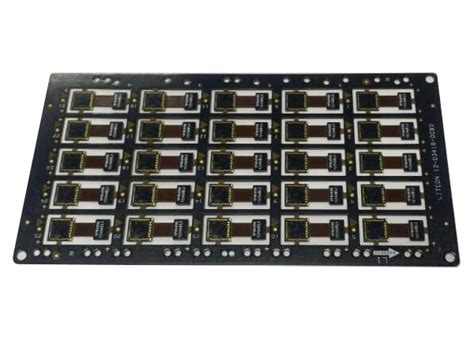
What Are The Advantages Of Using A 6-Layer PCB?
1. Increased Circuit Density
One of the main advantages of using a 6-layer PCB is the increased circuit density. With six layers available for routing traces, designers can pack more components and circuitry into a smaller space. This is especially important for devices that require miniaturization, such as smartphones, wearables, and IoT devices.
2. Improved Signal Integrity
6-layer PCBs offer improved signal integrity compared to boards with fewer layers. By separating power and ground planes, as well as using dedicated layers for critical signals, designers can minimize crosstalk, noise, and electromagnetic interference (EMI). This results in cleaner and more stable signals, which is crucial for high-speed applications like networking equipment and data centers.
3. Enhanced Thermal Management
The additional layers in a 6-layer PCB provide more surface area for heat dissipation. This is particularly important for power-hungry components like processors, FPGAs, and RF modules. By efficiently spreading heat across the board, 6-layer PCBs can prevent overheating and improve the overall reliability of the device.
What Are The Typical Layer Stackup For A 6-Layer PCB?
A typical 6-layer PCB stackup consists of the following layers:
| Layer | Function |
|---|---|
| Top Layer | Signal routing, components placement |
| Ground Layer | Ground reference plane |
| Inner Layer 1 | Signal routing |
| Inner Layer 2 | Signal routing |
| Power Layer | Power distribution |
| Bottom Layer | Signal routing, components placement |
The ground and power layers serve as reference planes and help to reduce EMI and crosstalk. The inner layers are used for additional signal routing, allowing for more complex circuitry and higher component density.
What Are The Design Considerations For 6-Layer PCBs?
When designing a 6-layer PCB, there are several key considerations to keep in mind:
1. Layer Stackup
Choosing the right layer stackup is crucial for optimizing signal integrity and power distribution. Designers must carefully consider the placement of power and ground planes, as well as the spacing between layers to minimize crosstalk and impedance issues.
2. Via Placement
Vias are used to interconnect traces between layers. Proper via placement is essential for maintaining signal integrity and preventing manufacturing issues. Designers should follow best practices for via sizing, spacing, and landing pad design to ensure reliable connections.
3. Trace Width And Spacing
The width and spacing of traces on a 6-layer PCB must be carefully calculated based on the required impedance, current carrying capacity, and manufacturing tolerances. Designers should use simulation tools to optimize trace geometry and ensure that the board meets performance and reliability requirements.

What Are The Manufacturing Challenges For 6-Layer PCBs?
Manufacturing 6-layer PCBs presents several challenges compared to simpler boards:
1. Registration Accuracy
Aligning the layers during the lamination process requires high precision to ensure proper registration. Any misalignment can result in open or short circuits, compromising the board’s functionality.
2. Drilling And Plating
Drilling and plating through-holes on a 6-layer PCB is more challenging due to the increased board thickness. Specialized equipment and processes are required to ensure clean and reliable hole walls and avoid defects like voids or breakouts.
3. Inspection And Testing
Inspecting and testing 6-layer PCBs is more complex due to the hidden inner layers. Advanced techniques like X-ray inspection and automated optical inspection (AOI) are often used to detect defects and ensure the board meets quality standards.
What Are The Applications Of 6-Layer PCBs?
6-layer PCBs are used in a wide range of applications that require high performance, reliability, and compact design. Some examples include:
- Smartphones and tablets
- Wearable devices
- IoT sensors and gateways
- Networking equipment (routers, switches)
- Data centers and servers
- Automotive electronics
- Medical devices
- Aerospace and defense systems
Frequently Asked Questions (FAQ)
1. What is the difference between a 4-layer and 6-layer PCB?
A 4-layer PCB has four conductive layers (top, bottom, and two inner layers), while a 6-layer PCB has six conductive layers (top, bottom, and four inner layers). The additional layers in a 6-layer PCB provide more space for routing traces and improved signal integrity.
2. Can I convert my 4-layer PCB design to a 6-layer PCB?
Yes, it is possible to convert a 4-layer PCB design to a 6-layer PCB. However, this requires a redesign of the circuit to take advantage of the additional layers and optimize the layer stackup. It is essential to work with experienced PCB designers to ensure a successful transition.
3. Are 6-layer PCBs more expensive than 4-layer PCBs?
Yes, 6-layer PCBs are generally more expensive than 4-layer PCBs due to the increased complexity of manufacturing and the additional materials required. However, the cost difference may be justified for applications that require the enhanced performance and reliability offered by 6-layer boards.
4. What are the typical lead times for manufacturing 6-layer PCBs?
Lead times for 6-layer PCBs can vary depending on the complexity of the design, the chosen manufacturer, and the order quantity. Typical lead times range from 2-4 weeks, but expedited options may be available for urgent projects.
5. What are the minimum trace width and spacing for 6-layer PCBs?
The minimum trace width and spacing for 6-layer PCBs depend on the manufacturing capabilities of the chosen PCB fabricator and the specific design requirements. Typical minimum trace width and spacing for 6-layer PCBs range from 3-4 mils (0.075-0.1 mm), but more advanced manufacturers may offer even finer features.
In conclusion, 6-layer PCBs offer numerous advantages over simpler boards, including increased circuit density, improved signal integrity, and enhanced thermal management. However, designing and manufacturing these complex boards requires careful consideration of layer stackup, via placement, trace geometry, and manufacturing challenges. By understanding the key aspects of 6-layer PCBs, designers can leverage their benefits to create high-performance, reliable, and compact electronic devices for a wide range of applications.


Leave a Reply