Introduction to PCB fabrication
Printed Circuit Board (PCB) fabrication is a crucial process in the electronics industry. It involves the creation of a board that connects electronic components using conductive tracks, pads, and other features etched from copper sheets laminated onto a non-conductive substrate. The quality and speed of PCB fabrication can significantly impact the performance and reliability of electronic devices.
In this article, we will explore the various aspects of fast and quality PCB fabrication, including the manufacturing process, materials used, design considerations, and quality control measures.
The PCB Fabrication Process
Step 1: PCB Design and Layout
The first step in PCB fabrication is the design and layout of the circuit board. This involves creating a schematic diagram of the electronic circuit and translating it into a physical layout using PCB design software. The layout determines the placement of components, routing of traces, and the overall size and shape of the board.
Step 2: Material Selection
The choice of materials is crucial for the performance and reliability of the PCB. The most common substrate material is FR-4, a glass-reinforced epoxy laminate. Other materials, such as polyimide or ceramic, may be used for high-temperature or high-frequency applications.
The copper foil used for the conductive layers comes in various thicknesses, typically ranging from 0.5 oz to 2 oz per square foot.
Step 3: Fabrication
The actual fabrication process involves several sub-steps:
-
Copper Clad Laminate: The substrate material is laminated with a thin layer of copper foil on one or both sides.
-
Drilling: Holes are drilled through the board to accommodate through-hole components and vias.
-
Plating: The drilled holes are plated with copper to create electrical connections between layers.
-
Patterning: The copper foil is patterned using a photolithographic process. A photoresist layer is applied, exposed to UV light through a photomask, and developed to reveal the desired pattern.
-
Etching: The exposed copper is etched away using a chemical solution, leaving only the desired traces and pads.
-
Soldermask Application: A soldermask layer is applied to protect the copper traces and prevent solder bridging.
-
Silkscreen Printing: A silkscreen layer is printed on the board to add labels, logos, and other markings.
-
Surface Finish: A surface finish, such as HASL (Hot Air Solder Leveling), ENIG (Electroless Nickel Immersion Gold), or OSP (Organic Solderability Preservative), is applied to protect the exposed copper and enhance solderability.
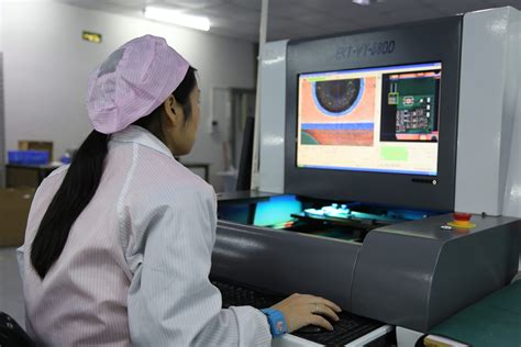
Step 4: Quality Control
Throughout the fabrication process, various quality control measures are implemented to ensure the reliability and consistency of the PCBs. These include:
- Visual inspection
- Electrical testing
- Microsectioning
- Contamination testing
- Thermal stress testing

PCB Materials
The choice of materials is critical for the performance and reliability of the PCB. Here are some common materials used in PCB fabrication:
| Material | Description | Applications |
|---|---|---|
| FR-4 | Glass-reinforced epoxy laminate | General-purpose PCBs |
| Polyimide | High-temperature and flexible substrate | Aerospace, military, and medical devices |
| Ceramic | High-frequency and high-temperature substrate | RF and microwave circuits |
| Aluminum | Metal-core substrate for heat dissipation | LED lighting and power electronics |
| Rogers | High-frequency and low-loss substrate | Wireless communication and radar systems |

Design Considerations for Fast and Quality PCB Fabrication
To ensure fast and quality PCB fabrication, designers must consider several factors:
1. Design for Manufacturability (DFM)
DFM guidelines help optimize the PCB layout for the fabrication process. This includes:
- Minimum trace width and spacing
- Minimum hole size and spacing
- Copper balancing
- Soldermask and silkscreen clearances
2. Material Selection
Choosing the appropriate substrate material and copper thickness based on the application requirements, such as temperature range, frequency, and mechanical stress.
3. Signal Integrity
Proper routing techniques and impedance control to minimize signal distortion, crosstalk, and electromagnetic interference (EMI).
4. Thermal Management
Designing for efficient heat dissipation, especially for high-power components, using techniques such as thermal vias, copper pours, and metal-core substrates.
5. Panelization
Optimizing the PCB panel layout to maximize fabrication efficiency and minimize material waste.

Quality Control in PCB Fabrication
Quality control is essential to ensure that the fabricated PCBs meet the required specifications and performance standards. Here are some common quality control measures:
| Quality Control Measure | Description |
|---|---|
| Visual Inspection | Checking for surface defects, such as scratches, dents, or discoloration |
| Electrical Testing | Verifying the continuity, isolation, and functionality of the PCB |
| Microsectioning | Cross-sectioning the PCB to inspect the internal layers and plated through-holes |
| Contamination Testing | Checking for ionic contamination on the PCB surface |
| Thermal Stress Testing | Subjecting the PCB to temperature cycling to assess its reliability under thermal stress |
Benefits of Fast and Quality PCB Fabrication
Fast and quality PCB fabrication offers several benefits for electronic product development and manufacturing:
-
Reduced Time-to-Market: Faster fabrication times enable quicker prototyping and shorter product development cycles.
-
Improved Reliability: High-quality PCBs with robust design and manufacturing processes ensure better product reliability and reduced field failures.
-
Cost Savings: Efficient fabrication processes and minimized material waste lead to lower production costs.
-
Enhanced Performance: Properly designed and fabricated PCBs offer better signal integrity, thermal management, and overall system performance.
Frequently Asked Questions (FAQ)
1. What is the typical turnaround time for PCB fabrication?
The turnaround time for PCB fabrication depends on various factors, such as the complexity of the design, the chosen materials, and the fabrication facility’s workload. Typical turnaround times range from 24 hours for simple, quick-turn prototypes to 1-2 weeks for more complex, high-volume production runs.
2. What are the most common PCB Surface Finishes?
The most common PCB surface finishes include:
- HASL (Hot Air Solder Leveling)
- ENIG (Electroless Nickel Immersion Gold)
- OSP (Organic Solderability Preservative)
- Immersion Silver
- Immersion Tin
Each surface finish has its advantages and disadvantages in terms of cost, durability, and solderability.
3. What is the minimum feature size achievable in PCB fabrication?
The minimum feature size depends on the fabrication facility’s capabilities and the chosen manufacturing process. Typical minimum feature sizes are:
- 4 mil (0.1 mm) trace width and spacing for standard PCBs
- 2 mil (0.05 mm) trace width and spacing for advanced PCBs
- 1 mil (0.025 mm) trace width and spacing for ultra-Fine Pitch PCBs
4. How can I ensure my PCB design is manufacturable?
To ensure your PCB design is manufacturable, follow these guidelines:
- Adhere to the fabrication facility’s design rules and DFM guidelines
- Use standard sizes and shapes for pads and holes
- Maintain proper trace width and spacing for the chosen copper thickness
- Balance copper distribution across the layers
- Avoid acute angles and sharp corners in trace routing
- Use vias sparingly and with appropriate size and spacing
5. What is the difference between a prototype PCB and a production PCB?
Prototype PCBs are typically fabricated in small quantities (1-10 pieces) to validate the design and functionality before mass production. They may have looser tolerances and use quicker fabrication processes to reduce turnaround time.
Production PCBs are fabricated in larger quantities (100+ pieces) using optimized processes to ensure consistency, reliability, and cost-effectiveness. They follow stricter tolerances and undergo more rigorous quality control measures.
Conclusion
Fast and quality PCB fabrication is essential for the success of electronic products in today’s competitive market. By understanding the fabrication process, selecting appropriate materials, and following design best practices, designers can ensure their PCBs are manufactured efficiently and meet the required performance standards.
As technology advances, PCB fabrication capabilities continue to improve, enabling the creation of more complex, high-density, and high-performance electronic devices. Staying up-to-date with the latest fabrication techniques and quality control measures is crucial for designers and manufacturers to stay competitive in the ever-evolving electronics industry.


Leave a Reply