Introduction to Fine Pitch PCB
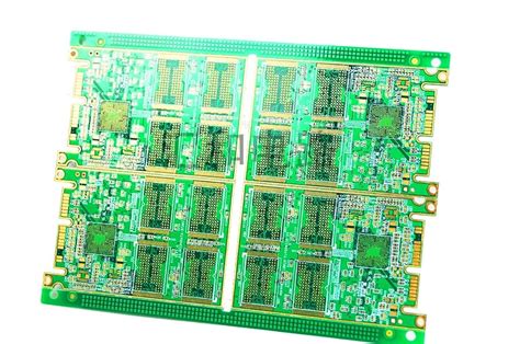
Fine pitch PCB, also known as high-density interconnect (HDI) PCB, is a type of printed circuit board that features smaller component pitch and higher wiring density compared to traditional PCBs. The term “pitch” refers to the distance between the centers of two adjacent pins or leads on a component. In fine pitch PCBs, this distance is typically less than 0.5mm (20 mils).
The demand for fine pitch PCBs has increased significantly in recent years due to the miniaturization of electronic devices and the need for more functionality in smaller form factors. Fine pitch PCBs are commonly used in applications such as smartphones, wearables, medical devices, and aerospace systems.
Advantages of Fine Pitch PCB
- Miniaturization: Fine pitch PCBs allow for smaller component sizes and higher component density, enabling the design of more compact electronic devices.
- Improved functionality: With the ability to accommodate more components and interconnects, fine pitch PCBs can support more complex and feature-rich designs.
- Enhanced signal integrity: The reduced pitch and trace widths in fine pitch PCBs minimize signal reflections and crosstalk, leading to improved signal integrity and higher-speed performance.
- Cost-effectiveness: Although the initial design and manufacturing costs may be higher, fine pitch PCBs can result in overall cost savings by reducing the size and weight of the end product.
Challenges in Fine Pitch PCB Design and Assembly
- Design complexity: Fine pitch PCBs require careful design considerations to ensure proper signal routing, impedance control, and thermal management.
- Manufacturing limitations: The smaller features in fine pitch PCBs demand higher precision in the manufacturing process, including tighter tolerances and more advanced equipment.
- Assembly challenges: The reduced pitch and smaller component sizes make the assembly process more difficult, requiring specialized equipment and techniques to ensure reliable connections.
- Inspection and testing: Traditional inspection and testing methods may not be suitable for fine pitch PCBs, necessitating the use of advanced techniques such as X-ray inspection and flying probe testing.
Fine Pitch PCB Design Considerations
Component Selection
When designing a fine pitch PCB, it is crucial to select components that are compatible with the desired pitch and packaging style. Some common fine pitch component packages include:
- Quad Flat No-lead (QFN): A surface-mount package with leads on all four sides of the component, featuring a pitch ranging from 0.4mm to 0.5mm.
- Ball Grid Array (BGA): A surface-mount package with a grid of solder balls underneath the component, offering pitches as low as 0.3mm.
- Chip Scale Package (CSP): A package with dimensions close to the die size, typically featuring a pitch of 0.5mm or less.
When selecting components, designers should also consider the thermal characteristics and power requirements to ensure proper heat dissipation and power delivery.
PCB Stack-up and Material Selection
The PCB stack-up and material selection play a significant role in the performance and manufacturability of fine pitch PCBs. Some key considerations include:
- Dielectric constant (Dk) and dissipation factor (Df): Choose materials with low Dk and Df values to minimize signal loss and improve signal integrity.
- Copper weight: Use appropriate copper weights for the desired trace widths and current carrying capacity, considering the skin effect at high frequencies.
- Laminate thickness: Thinner laminates can help reduce the overall PCB thickness and improve high-speed performance but may require more careful handling during manufacturing.
- Impedance control: Select materials and stack-up configurations that allow for accurate impedance control, particularly for high-speed signals.
| Material | Dielectric Constant (Dk) | Dissipation Factor (Df) | Typical Applications |
|---|---|---|---|
| FR-4 | 4.2 – 4.5 | 0.02 – 0.03 | General-purpose |
| Rogers 4350B | 3.48 | 0.0037 | High-frequency, RF |
| Isola I-Tera MT | 3.45 | 0.0031 | High-speed digital |
| Nelco N4000-13 SI | 3.7 | 0.009 | Automotive, aerospace |
Routing and Trace Width Considerations
Proper routing and trace width selection are essential for maintaining signal integrity and ensuring manufacturability in fine pitch PCBs. Some guidelines include:
- Minimize trace lengths: Keep traces as short as possible to reduce signal reflections and attenuation.
- Avoid sharp angles: Use 45-degree angles or curved traces instead of 90-degree angles to minimize signal reflections.
- Maintain consistent trace widths: Use consistent trace widths for each signal layer to ensure controlled impedance and minimize signal distortions.
- Use appropriate via sizes: Select via sizes that are compatible with the trace widths and pitch, considering the aspect ratio and drill size limitations.
| Trace Width (mm) | Impedance (Ω) | Current Capacity (A) |
|---|---|---|
| 0.1 | 90 – 120 | 0.5 – 0.8 |
| 0.15 | 70 – 100 | 0.8 – 1.2 |
| 0.2 | 60 – 90 | 1.2 – 1.8 |
| 0.25 | 50 – 80 | 1.8 – 2.5 |
Signal Integrity and EMI/EMC Considerations
Signal integrity and electromagnetic interference/compatibility (EMI/EMC) are critical concerns in fine pitch PCB design. Some strategies to address these issues include:
- Use ground planes: Incorporate ground planes to provide a low-impedance return path for high-speed signals and shield against EMI.
- Implement power planes: Use power planes to distribute power evenly across the PCB and minimize voltage drops and noise.
- Apply decoupling capacitors: Place decoupling capacitors close to power pins to suppress high-frequency noise and maintain signal integrity.
- Employ shielding techniques: Use shielding cans, conductive gaskets, or conformal shielding to minimize EMI and crosstalk between components.

Fine Pitch PCB Assembly Process
Solder Paste Printing
Solder paste printing is the first step in the fine pitch PCB assembly process. Due to the smaller pitch and component sizes, a high-precision stencil and printing process are required. Some key considerations include:
- Stencil thickness: Use a thinner stencil (typically 100-150 μm) to achieve the required solder paste volume and prevent bridging.
- Aperture design: Optimize the aperture size and shape to ensure consistent solder paste deposition and prevent solder balling or insufficient filling.
- Printing parameters: Control the printing speed, pressure, and separation speed to achieve a clean and uniform solder paste print.
- Stencil cleaning: Regularly clean the stencil to prevent solder paste buildup and maintain print quality.
Component Placement
Accurate component placement is crucial for fine pitch PCBs to ensure proper alignment and prevent shorts or opens. Some guidelines include:
- Use vision systems: Employ high-resolution cameras and vision systems to verify component alignment and detect placement errors.
- Implement pick-and-place machines: Use high-precision pick-and-place machines with fine pitch nozzles to accurately place components on the PCB.
- Control placement pressure: Adjust the placement pressure to prevent component damage or shifting while ensuring adequate contact with the solder paste.
- Verify placement accuracy: Conduct post-placement inspections to verify component alignment and correct any errors before reflow.
Reflow Soldering
Reflow soldering is the process of melting the solder paste to form a permanent connection between the components and the PCB. For fine pitch PCBs, the reflow profile must be carefully controlled to ensure proper solder joint formation and minimize defects. Some considerations include:
- Reflow profile optimization: Develop a reflow profile that accounts for the specific requirements of the solder paste, components, and PCB material, considering factors such as ramp rates, peak temperature, and time above liquidus.
- Nitrogen atmosphere: Use a nitrogen reflow environment to reduce oxidation and improve solder joint quality, particularly for lead-free solder alloys.
- Cooling rate control: Control the cooling rate to minimize thermal shock and prevent component or PCB damage.
- Reflow soldering defects: Monitor and address common reflow soldering defects, such as bridging, tombstoning, or insufficient wetting, through process optimization and control.
Inspection and Testing
Inspection and testing are essential for ensuring the quality and reliability of fine pitch PCB assemblies. Some common techniques include:
- Automated Optical Inspection (AOI): Use AOI systems to detect surface-level defects, such as missing components, misalignments, or solder bridges.
- X-ray Inspection: Employ X-ray inspection to examine solder joint quality and detect hidden defects, such as voids or insufficient solder fillets, particularly for BGA and QFN components.
- In-Circuit Testing (ICT): Perform electrical testing using an ICT system to verify the functionality and connectivity of the assembled PCB.
- Functional Testing: Conduct final functional testing to ensure that the assembled PCB meets the required performance specifications and operating conditions.

Frequently Asked Questions (FAQ)
-
Q: What is the minimum pitch that can be achieved with fine pitch PCBs?
A: The minimum pitch achievable in fine pitch PCBs depends on various factors, such as the manufacturing capabilities, component availability, and design requirements. Currently, pitches as low as 0.3mm (12 mils) are possible with advanced manufacturing techniques and specialized components. -
Q: Can fine pitch PCBs be assembled using traditional soldering methods?
A: While traditional soldering methods, such as wave soldering or hand soldering, can be used for fine pitch PCBs, they may not provide the required accuracy and consistency. Reflow soldering is the preferred method for fine pitch PCB assembly, as it offers better control over the solder joint formation and minimizes the risk of defects. -
Q: Are there any specific cleaning requirements for fine pitch PCBs?
A: Yes, fine pitch PCBs require thorough cleaning to remove flux residues and contaminants that can adversely affect the performance and reliability of the assembly. Due to the smaller pitch and component sizes, specialized cleaning agents and processes, such as ultrasonic cleaning or vapor degreasing, may be necessary to ensure effective cleaning without damaging the components or solder joints. -
Q: How can designers address the thermal management challenges in fine pitch PCBs?
A: Thermal management is a critical consideration in fine pitch PCB design, as the higher component density and smaller sizes can lead to increased heat generation and dissipation challenges. Designers can address these challenges by: - Selecting components with low thermal resistance and optimized packaging
- Using thermal vias and heat sinks to provide efficient heat dissipation paths
- Incorporating thermal interface materials (TIMs) to enhance heat transfer between components and heat sinks
-
Optimizing the PCB layout and airflow to promote effective cooling
-
Q: What are the key considerations for panelization in fine pitch PCB manufacturing?
A: Panelization is the process of arranging multiple PCB designs on a single panel for efficient manufacturing and assembly. For fine pitch PCBs, panelization considerations include: - Minimizing the panel border and inter-PCB spacing to maximize the number of PCBs per panel
- Using appropriate tab and route designs to ensure clean and accurate depanelization
- Incorporating fiducial markers and tooling holes for precise alignment and registration during assembly
- Balancing the panel layout to minimize warpage and ensure consistent processing across the panel

Conclusion
Fine pitch PCBs offer numerous advantages, such as miniaturization, improved functionality, and enhanced signal integrity, making them essential for modern electronic devices and systems. However, designing and assembling fine pitch PCBs presents unique challenges that require careful consideration and specialized techniques.
By understanding the key design considerations, such as component selection, PCB stack-up and material choice, routing and trace width optimization, and signal integrity management, designers can create fine pitch PCBs that meet the demanding requirements of today’s applications.
Moreover, implementing appropriate assembly processes, including high-precision solder paste printing, accurate component placement, controlled reflow soldering, and thorough inspection and testing, is crucial for ensuring the quality and reliability of fine pitch PCB assemblies.
As electronic devices continue to evolve and push the boundaries of miniaturization and performance, the importance of fine pitch PCBs will only continue to grow. By staying informed about the latest advancements in fine pitch PCB design and assembly techniques, engineers and manufacturers can remain at the forefront of this exciting and dynamic field.


Leave a Reply