Introduction to PCB PTH Technology
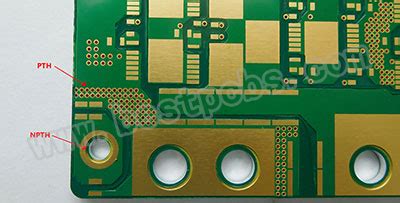
Plated through hole (PTH) is a vital technology in the fabrication of printed circuit boards (PCBs). It involves creating holes in a PCB and then plating them with a conductive material, typically copper, to establish electrical connections between different layers of the board. PTH has been a cornerstone of PCB manufacturing for decades, enabling the creation of reliable and robust electronic devices across various industries.
The Importance of PTH in PCB Design and Manufacturing
PTH plays a crucial role in PCB design and manufacturing for several reasons:
- Electrical Connectivity: PTH provides a means to connect different layers of a PCB, allowing for the creation of complex, multi-layer designs.
- Mechanical Strength: Plated through holes offer mechanical support to components mounted on the PCB, ensuring they remain securely attached to the board.
- Thermal Management: PTH can help dissipate heat from components by providing a thermal path through the board.
- Compatibility: Many electronic components, such as through-hole resistors and capacitors, rely on PTH for their mounting and connection to the PCB.
The PTH Manufacturing Process
The process of creating plated through holes involves several steps, each of which must be carried out with precision to ensure the quality and reliability of the final product.
Step 1: Drilling
The first step in the PTH process is drilling holes in the PCB substrate. This is typically done using high-speed, computer-controlled drill machines capable of creating holes with diameters ranging from 0.1mm to over 6mm. The drilling process must be carefully controlled to ensure the holes are positioned accurately and have consistent diameters.
Step 2: Deburring and Cleaning
After drilling, the holes must be deburred to remove any rough edges or debris that could interfere with the plating process. This is typically done using a chemical or mechanical deburring process. The board is then thoroughly cleaned to remove any contaminants that could affect the adhesion of the plating.
Step 3: Electroless Copper Deposition
The next step is to deposit a thin layer of copper inside the holes using an electroless plating process. This involves immersing the board in a copper plating solution, which deposits a thin, uniform layer of copper on the walls of the holes and the surface of the board. This layer serves as a conductive base for the subsequent electrolytic plating process.
Step 4: Electrolytic Copper Plating
After the electroless copper deposition, the board undergoes an electrolytic plating process to build up the thickness of the copper in the holes and on the surface of the board. This involves passing an electric current through the board while it is immersed in a copper plating solution. The thickness of the copper plating can be controlled by adjusting the current and the duration of the plating process.
Step 5: Resist Application and Patterning
Once the holes are plated, a photoresist is applied to the surface of the board and patterned using photolithography. This creates a protective mask that defines the areas where the copper will remain on the surface of the board.
Step 6: Etching and Resist Removal
The board is then etched to remove the unwanted copper, leaving only the desired circuit pattern and the plated through holes. Finally, the remaining photoresist is removed, and the board is cleaned and inspected for quality control.

Advantages of PTH in PCB Fabrication
PTH offers several advantages in PCB fabrication:
- Reliability: PTH provides a robust and reliable means of connecting different layers of a PCB, ensuring the integrity of the electrical connections over the life of the product.
- Versatility: PTH can be used with a wide range of PCB Materials and thicknesses, making it a versatile choice for various applications.
- Compatibility: PTH is compatible with many standard electronic components, such as through-hole resistors and capacitors, making it easy to design and assemble PCBs using these components.
- Thermal Management: The plated through holes can help dissipate heat from components, improving the thermal management of the PCB.

Challenges and Considerations in PTH PCB Fabrication
While PTH is a well-established and reliable technology, there are some challenges and considerations to keep in mind when designing and manufacturing PCBs with plated through holes.
Hole Size and Aspect Ratio
One of the main challenges in PTH PCB fabrication is achieving reliable plating in holes with high aspect ratios (the ratio of the hole depth to its diameter). As PCBs become thinner and more compact, the aspect ratios of the holes increase, making it more difficult to achieve uniform plating. This can lead to issues such as voids or thin spots in the plating, which can compromise the electrical and mechanical integrity of the connection.
To mitigate this, designers must carefully consider the hole sizes and aspect ratios when creating the PCB Layout. In some cases, it may be necessary to use larger hole diameters or to limit the number of layers in the board to ensure reliable plating.
Material Selection
The choice of PCB material can also impact the PTH process. Some materials, such as high-frequency laminates or those with low thermal expansion coefficients, can be more challenging to drill and plate. Designers must take these material properties into account and work closely with the PCB fabricator to ensure the manufacturability of the design.
Copper Thickness and Plating Quality
The thickness and quality of the copper plating in the holes are critical factors in the performance and reliability of the PCB. Insufficient plating thickness can lead to weak connections or even open circuits, while excessive plating can cause issues with component fit or lead to stress on the PCB substrate.
To ensure the right plating thickness and quality, PCB fabricators must carefully control the plating process parameters, such as the current density, temperature, and duration. They must also implement strict quality control measures, such as cross-sectional analysis and electrical testing, to verify the plating meets the specified requirements.

Alternative Technologies to PTH
While PTH remains a widely used technology in PCB fabrication, there are some alternatives that can be used in certain applications.
Surface Mount Technology (SMT)
Surface mount technology (SMT) involves mounting components directly on the surface of the PCB without the need for through holes. SMT components are smaller and can be placed more densely on the board, enabling the creation of more compact and lightweight designs.
However, SMT does not provide the same level of mechanical strength and thermal management as PTH, and it may not be suitable for all applications or components.
Blind and Buried Vias
Blind and buried vias are a type of interconnect that can be used as an alternative to PTH in some cases. A blind via is a hole that starts on one surface of the PCB and terminates at an inner layer, while a buried via is a hole that connects two or more inner layers without reaching either surface of the board.
Blind and buried vias can help reduce the overall thickness of the PCB and improve signal integrity by reducing the length of the interconnects. However, they are more complex and costly to manufacture than traditional PTH, and they may not be suitable for all designs or applications.
Future Trends in PTH PCB Fabrication
As electronic devices continue to become smaller, more complex, and more performance-driven, the demands on PCB fabrication technologies, including PTH, will continue to evolve. Some of the key trends and developments in PTH PCB fabrication include:
High Density Interconnect (HDI)
High density interconnect (HDI) PCBs are becoming increasingly common in applications that require high component density and signal integrity, such as smartphones, wearables, and IoT devices. HDI PCBs often feature smaller hole sizes and higher aspect ratios than traditional PCBs, pushing the limits of PTH technology.
To meet these challenges, PCB fabricators are developing advanced drilling and plating techniques, such as laser drilling and pulse plating, to achieve reliable and consistent PTH in HDI boards.
Embedded Components
Embedded components, where electronic components are placed inside the layers of the PCB rather than on the surface, are another emerging trend in PCB design and fabrication. Embedded components can help reduce the size and weight of the PCB, improve signal integrity, and enhance thermal management.
However, embedding components also presents new challenges for PTH, as the holes must be drilled and plated around the embedded components without damaging them. This requires precise control of the drilling and plating processes and close collaboration between the PCB designer and fabricator.
Additive Manufacturing
Additive manufacturing, also known as 3D printing, is a promising technology for PCB fabrication that could potentially revolutionize the way PTH is created. With additive manufacturing, the PCB could be built up layer by layer, with the holes and interconnects formed as part of the printing process.
This could enable the creation of more complex and intricate PTH structures, as well as reduce the time and cost of PCB fabrication. However, additive manufacturing for PCBs is still in the early stages of development, and there are challenges to overcome in terms of material properties, resolution, and reliability.
Conclusion
Plated through hole (PTH) technology remains a critical aspect of PCB fabrication, providing a reliable and robust means of connecting different layers of the board and mounting components. While there are challenges and considerations to keep in mind when designing and manufacturing PCBs with PTH, the technology continues to evolve to meet the demands of increasingly complex and high-performance electronic devices.
As PCB designers and fabricators look to the future, trends such as HDI, embedded components, and additive manufacturing are likely to shape the development of PTH technology. By staying at the forefront of these trends and working closely together, designers and fabricators can ensure that PTH remains a vital and enabling technology for the electronics industry.
Frequently Asked Questions (FAQ)
-
What is the difference between PTH and SMT?
PTH (plated through hole) and SMT (surface mount technology) are two different methods of mounting components on a PCB. In PTH, the component leads are inserted into holes drilled in the board and then soldered, while in SMT, the components are placed directly on the surface of the board and soldered. PTH provides stronger mechanical connections and better thermal management, while SMT allows for higher component density and smaller board sizes. -
Can PTH be used with all types of PCB materials?
PTH can be used with a wide range of PCB materials, including FR-4, high-frequency laminates, and flexible substrates. However, some materials may be more challenging to drill and plate due to their physical properties, such as hardness or thermal expansion. Designers must consider the material characteristics when creating the PCB layout and work closely with the fabricator to ensure manufacturability. -
What is the minimum hole size for PTH?
The minimum hole size for PTH depends on several factors, including the PCB Thickness, aspect ratio, and plating requirements. In general, holes as small as 0.1mm in diameter can be reliably plated, but the aspect ratio (hole depth to diameter) should be kept below 10:1 to ensure consistent plating quality. For high-density designs or thicker boards, larger hole sizes or alternative technologies like blind and buried vias may be necessary. -
How is the quality of PTH evaluated?
The quality of PTH is typically evaluated through a combination of visual inspection, cross-sectional analysis, and electrical testing. Visual inspection checks for any surface defects or irregularities, while cross-sectional analysis involves cutting the board and examining the plating thickness and uniformity under a microscope. Electrical testing, such as continuity and resistance measurements, verifies the integrity of the electrical connections. PCB fabricators use these methods to ensure the PTH meets the specified requirements and performance criteria. -
What are the challenges in PTH PCB fabrication?
Some of the main challenges in PTH PCB fabrication include achieving reliable plating in holes with high aspect ratios, selecting compatible materials, controlling the plating thickness and quality, and managing the costs and lead times associated with the drilling and plating processes. As PCBs become more complex and miniaturized, these challenges are likely to become more pronounced, requiring continued innovation and collaboration between designers and fabricators to overcome them.
| PTH vs SMT | PTH | SMT |
|---|---|---|
| Component Mounting | Components are inserted into drilled holes and soldered | Components are placed directly on the surface and soldered |
| Mechanical Strength | Provides stronger mechanical connections | Offers less mechanical strength compared to PTH |
| Thermal Management | Allows for better thermal management through the holes | Limited thermal management capabilities |
| Component Density | Lower component density due to the space required for holes | Higher component density, enabling smaller board sizes |
| Cost and Assembly Speed | Generally slower and more costly due to drilling and plating process | Faster and more cost-effective for high-volume production |
| Suitability for Large Components | Well-suited for large, heavy components that require strong mounting | Less suitable for large components due to limited space on the surface |
| Aspect Ratio | Hole Diameter (mm) | PCB Thickness (mm) |
|---|---|---|
| 5:1 | 0.3 | 1.5 |
| 8:1 | 0.2 | 1.6 |
| 10:1 | 0.15 | 1.5 |
| 12:1 | 0.1 | 1.2 |
Table 2: Examples of PTH aspect ratios and corresponding hole diameters and PCB thicknesses.


Leave a Reply