Introduction to PTH PCB
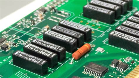
PTH PCB, or Plated Through Hole Printed Circuit Board, is a type of circuit board that features electroplated through holes. These holes allow electrical connections to be made between the different layers of the board, enabling more complex circuit designs and improved reliability. PTH PCBs are widely used in various electronic applications, from consumer devices to industrial equipment.
What is a PTH PCB?
A PTH PCB is a printed circuit board that has holes drilled through it, which are then electroplated with a conductive material, typically copper. This process creates electrical connections between the different layers of the board, allowing for more complex circuit designs and improved signal integrity. The plated through holes also provide mechanical support for components mounted on the board.
Advantages of PTH PCB
PTH PCBs offer several advantages over other types of circuit boards:
- Improved Reliability: The electroplated through holes provide a strong mechanical and electrical connection between layers, reducing the risk of connection failures.
- Better Signal Integrity: The plated through holes minimize signal loss and interference, ensuring cleaner signals and improved performance.
- Increased Density: PTH PCBs allow for more components to be mounted on a smaller board, enabling more compact designs.
- Enhanced Heat Dissipation: The plated through holes can also act as thermal vias, helping to dissipate heat from components more efficiently.
Manufacturing Process of PTH PCB
The manufacturing process of a PTH PCB involves several steps, each requiring precision and attention to detail. Here’s an overview of the main stages:
1. Designing the PCB
The first step is to design the PCB using specialized software. The design includes the circuit layout, component placement, and the location of the through holes. The design files are then used to create the photomasks needed for the subsequent steps.
2. Printing the Circuit Pattern
The circuit pattern is printed onto the copper-clad laminate using a photoresist and exposure to UV light. The exposed areas of the photoresist harden, while the unexposed areas are washed away, leaving the desired circuit pattern on the copper.
3. Etching the Copper
The exposed copper is then etched away using a chemical solution, typically ferric chloride or ammonium persulfate. This process removes the unwanted copper, leaving only the desired circuit pattern.
4. Drilling the Through Holes
The through holes are drilled using a computer-controlled drill machine. The drill bits used are typically made of tungsten carbide or diamond-tipped to ensure precise and clean holes.
5. Electroplating the Through Holes
The drilled holes are then electroplated with a conductive material, usually copper. This process involves several steps:
a. Cleaning: The board is cleaned to remove any debris and ensure good adhesion of the plating.
b. Activation: The holes are activated with a catalyst to promote the deposition of the plating material.
c. Electroless Copper Deposition: A thin layer of copper is deposited onto the holes using an electroless plating process.
d. Electrolytic Copper Plating: The board is then placed in an electrolytic plating bath, where a thicker layer of copper is deposited onto the holes and the circuit pattern.
6. Applying the Solder Mask and Silkscreen
A solder mask is applied to the board to protect the copper traces and prevent solder bridges. The silkscreen layer is then added to provide text and symbols for component placement and identification.
7. Surface Finishing
The final step is to apply a surface finish to the exposed copper areas to protect them from oxidation and improve solderability. Common surface finishes include:
– Hot Air Solder Leveling (HASL)
– Electroless Nickel Immersion Gold (ENIG)
– Immersion Silver
– Immersion Tin
| Surface Finish | Advantages | Disadvantages |
|---|---|---|
| HASL | – Low cost – Good solderability – Widely available |
– Uneven surface – Thermal shock to components |
| ENIG | – Flat surface – Excellent solderability – Long shelf life |
– Higher cost – Possible nickel corrosion |
| Immersion Silver | – Low cost – Good solderability – Flat surface |
– Limited shelf life – Possible silver migration |
| Immersion Tin | – Low cost – Good solderability – Flat surface |
– Limited shelf life – Possible tin whiskers |

Applications of PTH PCB
PTH PCBs are used in a wide range of electronic applications due to their reliability, signal integrity, and ability to accommodate high component density. Some common applications include:
1. Consumer Electronics
PTH PCBs are found in many consumer electronic devices, such as:
– Smartphones
– Laptops
– Televisions
– Home appliances
2. Automotive Electronics
In the automotive industry, PTH PCBs are used in various electronic systems, including:
– Engine control units (ECUs)
– Infotainment systems
– Driver assistance systems
– Powertrain control modules
3. Industrial Equipment
PTH PCBs are also used in industrial equipment, such as:
– Motor drives
– Power supplies
– Programmable logic controllers (PLCs)
– Human-machine interfaces (HMIs)
4. Medical Devices
In the medical field, PTH PCBs are used in a variety of devices, such as:
– Patient monitors
– Diagnostic equipment
– Imaging systems
– Implantable devices
5. Aerospace and Defense
PTH PCBs are essential in aerospace and defense applications, where reliability and performance are critical. Examples include:
– Avionics systems
– Radar and sonar equipment
– Satellite communication devices
– Missile guidance systems

Factors Affecting PTH PCB Performance
Several factors can impact the performance and reliability of PTH PCBs:
1. Material Selection
The choice of materials used in the construction of a PTH PCB can significantly affect its performance. Key considerations include:
– Laminate material (e.g., FR-4, Rogers, polyimide)
– Copper weight and thickness
– Solder mask and silkscreen materials
2. Hole Quality
The quality of the drilled holes is crucial for the reliability of the electrical connections. Factors that can affect hole quality include:
– Drill bit wear and breakage
– Drilling speed and feed rate
– Hole wall roughness and smear
3. Plating Quality
The quality of the electroplated through holes directly impacts the electrical and mechanical integrity of the board. Factors that can affect plating quality include:
– Plating thickness and uniformity
– Plating adhesion
– Plating voids and nodules
4. Circuit Design
The circuit design itself can also affect the performance of a PTH PCB. Key considerations include:
– Trace width and spacing
– Component placement and orientation
– Signal integrity and EMI/EMC
5. Manufacturing Process Control
Strict process control during the manufacturing of PTH PCBs is essential to ensure consistent quality and reliability. This includes monitoring and controlling:
– Environmental conditions (temperature, humidity)
– Chemical concentrations and purity
– Equipment calibration and maintenance

Future Trends in PTH PCB Technology
As electronic devices continue to evolve and become more complex, PTH PCB technology must keep pace to meet the growing demands for performance, reliability, and miniaturization. Some of the future trends in PTH PCB technology include:
1. High-Density Interconnect (HDI) PCBs
HDI PCBs feature finer trace widths and smaller vias, allowing for higher component density and more complex circuit designs. This technology is becoming increasingly important in applications such as wearable devices, 5G communication systems, and advanced medical equipment.
2. Embedded Components
Embedding passive components (resistors, capacitors) within the layers of a PTH PCB can further increase component density and reduce the overall size of the board. This technology is particularly useful in applications where space is at a premium, such as implantable medical devices and aerospace systems.
3. Advanced Materials
The development of new laminate materials with improved thermal, mechanical, and electrical properties is ongoing. These materials, such as high-frequency laminates and low-loss dielectrics, are essential for meeting the demands of emerging technologies like 5G, IoT, and autonomous vehicles.
4. 3D Printing
3D printing technology is being explored as a potential method for fabricating PTH PCBs. This approach could enable faster prototyping, greater design flexibility, and the ability to create complex, three-dimensional circuit structures.
5. Environmental Sustainability
As environmental concerns continue to grow, there is an increasing focus on developing more sustainable and eco-friendly PCB manufacturing processes. This includes the use of lead-free solders, halogen-free laminates, and the adoption of green manufacturing practices to reduce waste and energy consumption.
Frequently Asked Questions (FAQ)
- What is the difference between a PTH PCB and an SMT PCB?
-
A PTH PCB uses through holes to mount components and make electrical connections between layers, while an SMT (Surface Mount Technology) PCB has components mounted directly onto the surface of the board without the need for through holes.
-
Can PTH and SMT components be used together on the same PCB?
-
Yes, it is common to have both PTH and SMT components on the same PCB. This is often referred to as a mixed-technology or hybrid PCB.
-
What is the minimum hole size that can be drilled in a PTH PCB?
-
The minimum hole size depends on the capabilities of the PCB manufacturer and the thickness of the board. Typically, the minimum hole size ranges from 0.2mm to 0.4mm in diameter.
-
How does the number of layers in a PTH PCB affect its performance?
-
Increasing the number of layers in a PTH PCB can improve signal integrity, reduce electromagnetic interference (EMI), and allow for more complex circuit designs. However, it also increases the cost and manufacturing complexity of the board.
-
What is the typical lifespan of a PTH PCB?
- The lifespan of a PTH PCB depends on various factors, such as the operating environment, power levels, and the quality of the manufacturing process. In general, a well-designed and manufactured PTH PCB can last for several decades under normal operating conditions.
Conclusion
PTH PCBs are a crucial component in the world of electronics, offering reliable electrical connections, good signal integrity, and the ability to accommodate high component density. The manufacturing process of PTH PCBs involves several precise steps, from designing the circuit layout to electroplating the through holes and applying the final surface finish.
As electronic devices continue to advance, PTH PCB technology must evolve to keep pace with the growing demands for performance, reliability, and miniaturization. Future trends in PTH PCB technology include the development of high-density interconnect (HDI) PCBs, embedded components, advanced materials, 3D printing, and a focus on environmental sustainability.
By understanding the fundamentals of PTH PCBs, their manufacturing process, applications, and future trends, engineers and designers can make informed decisions when developing new electronic products and systems. As the electronics industry continues to push the boundaries of what is possible, PTH PCBs will remain an essential building block for reliable, high-performance electronic devices.


Leave a Reply