Understanding High-Frequency PCBs
What is a High-Frequency PCB?
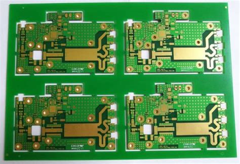
A high-frequency PCB is a printed circuit board that is specifically designed to handle high-frequency signals. These PCBs are engineered to minimize signal loss, distortion, and interference, which are common issues when dealing with high-frequency signals. They are manufactured using special materials and techniques to ensure optimal performance in high-frequency applications.
Key Characteristics of High-Frequency PCBs
High-frequency PCBs possess several distinct characteristics that set them apart from standard PCBs:
-
Low Dielectric Constant (Dk): High-frequency PCBs use substrate materials with low dielectric constants to minimize signal loss and distortion. Common materials include PTFE (Teflon), Rogers, and Isola.
-
Low Dissipation Factor (Df): The dissipation factor represents the amount of energy lost as heat in the substrate material. High-frequency PCBs require materials with low dissipation factors to minimize power loss and maintain signal integrity.
-
Controlled Impedance: To ensure proper signal transmission, high-frequency PCBs are designed with controlled impedance traces. This involves carefully selecting the trace width, thickness, and spacing to match the desired characteristic impedance.
-
Tight Tolerances: High-frequency PCBs require tighter manufacturing tolerances compared to standard PCBs. This includes precise control over trace widths, spacings, and hole sizes to maintain consistent performance.
Structure of High-Frequency PCBs
Substrate Materials
The choice of substrate material is crucial for high-frequency PCBs. The most commonly used materials include:
-
PTFE (Teflon): PTFE is known for its excellent dielectric properties, low loss tangent, and high thermal stability. It is often used in high-frequency applications up to 77 GHz.
-
Rogers: Rogers materials, such as RO4003C and RO4350B, offer a combination of low dielectric constant, low loss tangent, and good thermal stability. They are suitable for applications up to 40 GHz.
-
Isola: Isola materials, like IS400 and IS410, provide a balance of performance and cost-effectiveness. They are commonly used in high-frequency applications up to 10 GHz.
Copper Foil
High-frequency PCBs typically use copper foil with a thickness of 0.5 oz to 2 oz. The copper foil is laminated onto the substrate material to form the conductive layer. The choice of copper foil thickness depends on the specific application requirements, such as current carrying capacity and skin effect.
Multilayer Structures
High-frequency PCBs often employ multilayer structures to achieve desired functionality and performance. Multilayer boards consist of multiple conductive layers separated by dielectric layers. This allows for the integration of power and ground planes, as well as the routing of high-frequency signals on inner layers to minimize interference.
Via Technologies
Vias are used to interconnect different layers in a Multilayer PCB. In high-frequency PCBs, special via technologies are employed to minimize signal loss and reflections:
-
Blind Vias: Blind vias connect an outer layer to an inner layer without penetrating through the entire Board Thickness. They are used to reduce signal path length and minimize reflections.
-
Buried vias: Buried vias connect two or more inner layers without reaching the outer layers. They are used to create interconnections between inner layers while minimizing the impact on the outer layer routing.
-
Microvias: Microvias are small-diameter vias (typically less than 150 microns) that are used for high-density interconnects. They enable shorter signal paths and improved signal integrity in high-frequency designs.

Types of High-Frequency PCBs
Microstrip PCBs
Microstrip PCBs consist of a conductive trace on one side of the substrate, with a ground plane on the opposite side. The trace is exposed to the air, which acts as the dielectric medium. Microstrip PCBs are commonly used for high-frequency applications up to 10 GHz due to their simplicity and ease of fabrication.
| Characteristic | Value |
|---|---|
| Dielectric Constant (Dk) | 2.2 – 4.5 |
| Dissipation Factor (Df) | 0.001 – 0.02 |
| Trace Width | 0.1 mm – 1 mm |
| Substrate Thickness | 0.25 mm – 1.6 mm |
Stripline PCBs
Stripline PCBs have a conductive trace embedded between two ground planes within the substrate. The trace is completely surrounded by the dielectric material, which provides better shielding and reduces radiation compared to microstrip PCBs. Stripline PCBs are suitable for applications up to 20 GHz.
| Characteristic | Value |
|---|---|
| Dielectric Constant (Dk) | 2.2 – 4.5 |
| Dissipation Factor (Df) | 0.001 – 0.02 |
| Trace Width | 0.05 mm – 0.5 mm |
| Substrate Thickness | 0.25 mm – 1.6 mm |
Coplanar Waveguide (CPW) PCBs
Coplanar waveguide PCBs have a conductive trace and ground planes on the same side of the substrate. The trace is surrounded by the ground planes, which provide shielding and reduce crosstalk. CPW PCBs offer a wider bandwidth compared to microstrip and stripline PCBs, making them suitable for applications up to 40 GHz.
| Characteristic | Value |
|---|---|
| Dielectric Constant (Dk) | 2.2 – 4.5 |
| Dissipation Factor (Df) | 0.001 – 0.02 |
| Trace Width | 0.05 mm – 0.5 mm |
| Gap Width | 0.05 mm – 0.5 mm |
| Substrate Thickness | 0.25 mm – 1.6 mm |

Design Considerations for High-Frequency PCBs
Designing high-frequency PCBs requires careful consideration of several factors to ensure optimal performance:
-
Impedance Matching: Proper impedance matching is essential to minimize signal reflections and ensure efficient power transfer. The trace width, thickness, and spacing should be carefully calculated to achieve the desired characteristic impedance.
-
Signal Integrity: Signal integrity issues, such as crosstalk, reflections, and attenuation, become more pronounced at high frequencies. Careful layout techniques, such as proper grounding, shielding, and trace routing, should be employed to maintain signal integrity.
-
Power Distribution: Efficient power distribution is crucial in high-frequency PCBs to minimize noise and ensure stable operation. Power and ground planes should be properly designed, and decoupling capacitors should be strategically placed to reduce high-frequency noise.
-
Thermal Management: High-frequency PCBs often generate significant heat due to power dissipation. Proper thermal management techniques, such as the use of heatsinks, thermal vias, and temperature-resistant materials, should be employed to ensure reliable operation.
-
Manufacturing Considerations: High-frequency PCBs require precise manufacturing processes to maintain tight tolerances and ensure consistent performance. Close collaboration with the PCB manufacturer is essential to ensure that the design can be reliably manufactured and meets the required specifications.

Frequently Asked Questions (FAQ)
-
What is the difference between a high-frequency PCB and a standard PCB?
A high-frequency PCB is specifically designed to handle high-frequency signals, typically above 500 MHz. It uses specialized materials and techniques to minimize signal loss, distortion, and interference. Standard PCBs, on the other hand, are designed for lower frequency applications and may not have the same level of performance at high frequencies. -
What are the most common substrate materials used in high-frequency PCBs?
The most common substrate materials used in high-frequency PCBs are PTFE (Teflon), Rogers, and Isola. These materials have low dielectric constants, low loss tangents, and good thermal stability, making them suitable for high-frequency applications. -
What is the purpose of controlled impedance in high-frequency PCBs?
Controlled impedance is used in high-frequency PCBs to ensure proper signal transmission and minimize reflections. By carefully selecting the trace width, thickness, and spacing, the characteristic impedance of the traces can be matched to the desired value, typically 50 ohms or 75 ohms. -
What are the advantages of using blind and buried vias in high-frequency PCBs?
Blind and buried vias offer several advantages in high-frequency PCBs. Blind vias connect an outer layer to an inner layer without penetrating through the entire board thickness, reducing signal path length and minimizing reflections. Buried vias connect inner layers without reaching the outer layers, allowing for interconnections between inner layers while minimizing the impact on outer layer routing. -
How can signal integrity be maintained in high-frequency PCBs?
Signal integrity in high-frequency PCBs can be maintained through careful layout techniques. This includes proper grounding and shielding to reduce crosstalk and interference, strategic placement of decoupling capacitors to minimize high-frequency noise, and optimized trace routing to minimize reflections and attenuation. Simulation tools and analysis techniques can also be used to validate the design and ensure signal integrity.
Conclusion
High-frequency PCBs are essential for a wide range of applications that require the handling of high-frequency signals. These PCBs are designed using specialized materials and techniques to minimize signal loss, distortion, and interference. Understanding the structure and types of high-frequency PCBs, as well as the key design considerations, is crucial for engineers and designers working on high-frequency projects.
By selecting the appropriate substrate materials, employing advanced via technologies, and following best design practices, high-frequency PCBs can be optimized for performance, reliability, and manufacturability. As technology continues to advance and the demand for high-frequency applications grows, the importance of high-frequency PCBs will only continue to increase.


Leave a Reply