Introduction to High-Frequency PCBs
High-frequency printed circuit boards (PCBs) are specialized boards designed to operate at high frequencies, typically above 1 GHz. These PCBs are crucial components in various applications, including RF and microwave systems, telecommunications, aerospace, and defense industries. High-frequency PCBs require specific design considerations, materials, and manufacturing processes to ensure optimal performance and reliability.
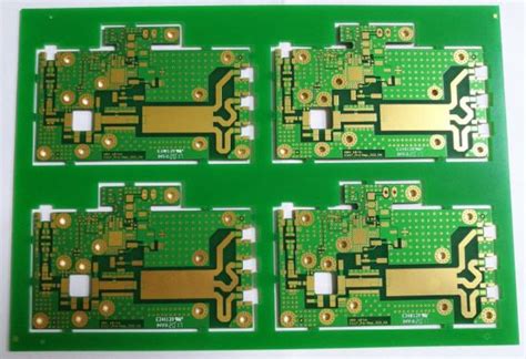
What Makes High-Frequency PCBs Different?
High-frequency PCBs differ from standard PCBs in several aspects:
-
Material Properties: High-frequency PCBs require materials with low dielectric constants and loss tangents to minimize signal loss and distortion at high frequencies. Common materials include PTFE (Polytetrafluoroethylene), Rogers, and Taconic.
-
Trace Geometry: Trace width, spacing, and length must be carefully controlled to maintain Impedance Matching and minimize signal reflections. High-frequency PCBs often employ controlled impedance traces and microstrip or stripline transmission lines.
-
Grounding and Shielding: Proper grounding and shielding techniques are essential to reduce electromagnetic interference (EMI) and crosstalk between signals. High-frequency PCBs often incorporate ground planes, via stitching, and shielding enclosures.
-
Manufacturing Processes: High-frequency PCBs require specialized manufacturing processes, such as advanced lamination, precision drilling, and selective plating, to ensure tight tolerances and high-quality finishes.
Designing High-Frequency PCBs
Material Selection
Choosing the right material is crucial for high-frequency PCB performance. The following table compares common high-frequency PCB materials:
| Material | Dielectric Constant | Loss Tangent | Thermal Stability | Cost |
|---|---|---|---|---|
| FR-4 | 4.4 | 0.02 | Low | Low |
| Rogers | 2.2 – 10.2 | 0.0009 – 0.0035 | High | High |
| Taconic | 2.1 – 3.0 | 0.0009 – 0.0030 | High | High |
| PTFE | 2.1 | 0.0002 | High | High |
When selecting materials, consider the following factors:
- Dielectric constant and loss tangent at the operating frequency
- Thermal stability and coefficient of thermal expansion (CTE)
- Cost and availability
- Compatibility with the manufacturing process
Trace Geometry and Impedance Control
Properly designing trace geometry and controlling impedance are essential for high-frequency PCBs. Key considerations include:
-
Trace Width and Spacing: Calculate trace width and spacing based on the desired characteristic impedance, substrate material properties, and layer stackup. Use Impedance Calculators or simulation tools to optimize trace geometry.
-
Transmission Lines: Use microstrip or stripline transmission lines for controlled impedance traces. Microstrip lines are exposed on the outer layers, while stripline traces are embedded between ground planes.
-
Trace Length Matching: Match the lengths of critical signal traces to minimize signal skew and ensure proper timing. Use serpentine routing or delay lines to adjust trace lengths.
-
Via Design: Minimize the use of vias, as they can introduce discontinuities and reflections. Use microvias or Buried vias when necessary, and optimize via geometry for impedance matching.
Grounding and Shielding
Effective grounding and shielding strategies are essential for high-frequency PCBs:
-
Ground Planes: Use uninterrupted ground planes to provide a low-impedance return path for high-frequency signals. Avoid splitting ground planes whenever possible.
-
Via Stitching: Use via stitching to connect ground planes on different layers, minimizing ground impedance and reducing EMI.
-
Shielding Enclosures: Incorporate shielding enclosures or cans to isolate sensitive components and reduce EMI. Use conductive gaskets or RF absorbers to improve shielding effectiveness.
-
Decoupling and Filtering: Use decoupling capacitors and filtering techniques to reduce power supply noise and high-frequency interference.

Manufacturing High-Frequency PCBs
Specialized Manufacturing Processes
High-frequency PCBs require specialized manufacturing processes to ensure high quality and performance:
-
Advanced Lamination: Use vacuum lamination or hydraulic press lamination to ensure uniform bonding and minimize air gaps between layers.
-
Precision Drilling: Employ high-speed, precision drilling machines to create small, accurate holes for vias and components. Use laser drilling for microvias.
-
Selective Plating: Use selective plating techniques, such as pattern plating or button plating, to deposit thicker copper in critical areas, improving signal integrity and thermal management.
-
Surface Finish: Choose an appropriate surface finish, such as immersion silver (IAg), immersion tin (ISn), or electroless nickel/immersion gold (ENIG), based on the application requirements and component compatibility.
Quality Control and Testing
Rigorous quality control and testing are essential for high-frequency PCBs:
-
Visual Inspection: Perform visual inspections to identify surface defects, such as scratches, dents, or discoloration.
-
Automated Optical Inspection (AOI): Use AOI machines to detect manufacturing defects, such as short circuits, open circuits, or missing components.
-
X-ray Inspection: Employ X-ray inspection to detect internal defects, such as voids, delamination, or misaligned vias.
-
Electrical Testing: Perform electrical tests, such as continuity, insulation resistance, and high-potential (HiPot) tests, to verify electrical performance and safety.
-
RF Testing: Conduct RF testing, such as S-parameter measurements or time-domain reflectometry (TDR), to characterize high-frequency performance and identify signal integrity issues.

One-Stop High-Frequency PCB Manufacturing
One-stop high-frequency PCB manufacturing offers several advantages for customers:
-
Streamlined Process: A one-stop manufacturer handles the entire PCB production process, from design to fabrication, assembly, and testing, simplifying the supply chain and reducing lead times.
-
Expertise and Experience: One-stop manufacturers have the expertise and experience to handle the unique challenges of high-frequency PCB design and manufacturing, ensuring optimal performance and reliability.
-
Customization and Flexibility: One-stop manufacturers can offer customized solutions tailored to specific application requirements, accommodating various materials, stackups, and feature sizes.
-
Cost Efficiency: By consolidating the manufacturing process under one roof, one-stop manufacturers can optimize costs and offer competitive pricing without compromising quality.
-
Rapid Prototyping: One-stop manufacturers often provide rapid prototyping services, enabling quick turnaround times for Prototype Boards and facilitating faster product development cycles.

Conclusion
High-frequency PCBs are essential components in various RF and microwave applications, requiring specialized design, materials, and manufacturing processes. By understanding the unique challenges and considerations involved in high-frequency PCB production, designers and manufacturers can ensure optimal performance, reliability, and cost-effectiveness. One-stop high-frequency PCB manufacturing offers a streamlined, efficient, and customizable solution for customers seeking high-quality boards for their specific applications.
Frequently Asked Questions (FAQ)
-
What is the difference between high-frequency PCBs and standard PCBs?
High-frequency PCBs are designed to operate at frequencies above 1 GHz, requiring specialized materials, trace geometries, and manufacturing processes to ensure optimal performance and signal integrity. Standard PCBs, on the other hand, are designed for lower-frequency applications and may not have the same stringent requirements. -
What materials are commonly used for high-frequency PCBs?
Common materials for high-frequency PCBs include PTFE (Polytetrafluoroethylene), Rogers, and Taconic. These materials have low dielectric constants and loss tangents, which are essential for minimizing signal loss and distortion at high frequencies. -
Why is impedance control important in high-frequency PCB design?
Impedance control is crucial in high-frequency PCB design to ensure proper signal transmission and minimize reflections. By maintaining a consistent characteristic impedance along the signal path, designers can prevent signal degradation, distortion, and interference. -
What are the benefits of using a one-stop high-frequency PCB manufacturer?
One-stop high-frequency PCB manufacturers offer a streamlined process, expertise, customization, cost efficiency, and rapid prototyping capabilities. By consolidating the entire manufacturing process under one roof, customers can benefit from faster lead times, optimized costs, and high-quality boards tailored to their specific application requirements. -
How can I ensure the quality and reliability of my high-frequency PCBs?
To ensure the quality and reliability of high-frequency PCBs, manufacturers employ rigorous quality control and testing procedures. These include visual inspections, automated optical inspection (AOI), X-ray inspection, electrical testing, and RF testing. By adhering to strict quality standards and performing comprehensive testing, manufacturers can deliver high-performance, reliable boards for demanding high-frequency applications.


Leave a Reply