What is a Flexible PCB?
A flexible PCB, also known as an FPC, is a type of printed circuit board that consists of a thin, flexible substrate made of materials such as polyimide or polyester. These substrates are laminated with conductive copper traces, allowing for electrical connectivity between components. FPCs can be single-sided, double-sided, or multi-layered, depending on the complexity of the design and the application requirements.
Advantages of Flexible PCBs
Flexible PCBs offer several advantages over traditional rigid PCBs, including:
- Flexibility: FPCs can bend, twist, and fold, enabling them to fit into tight spaces and conform to various shapes.
- Lightweight: Due to the thin substrate materials used, FPCs are significantly lighter than rigid PCBs, making them ideal for portable and wearable devices.
- Space-saving: FPCs can be folded and stacked, allowing for more compact designs and reducing the overall size of electronic devices.
- Durability: Despite their flexibility, FPCs are highly durable and can withstand repeated bending and flexing without compromising their functionality.
- High-density interconnects: FPCs can accommodate high-density interconnects, enabling the integration of more components and features in a smaller footprint.
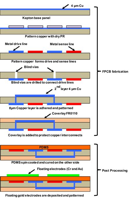
Fabricating FPC: The Manufacturing Process
The manufacturing process of flexible PCBs involves several key steps, each of which plays a crucial role in ensuring the quality and reliability of the final product. Let’s take a closer look at each step:
Step 1: Design and Artwork Creation
The first step in fabricating FPCs is to create the circuit design and artwork. This involves using specialized PCB design software to layout the conductive traces, components, and other features of the FPC. The designer must consider the flexibility requirements, bend radius, and overall dimensions of the FPC to ensure optimal performance and reliability.
Step 2: Material Selection
Once the design is finalized, the next step is to select the appropriate materials for the FPC. The most common substrate materials used in FPC manufacturing are polyimide and polyester. Polyimide is known for its excellent thermal stability, chemical resistance, and mechanical properties, making it the preferred choice for high-performance applications. Polyester, on the other hand, is a more cost-effective option suitable for less demanding applications.
The conductive traces on the FPC are typically made of copper, which is laminated onto the substrate material. The thickness of the copper layer can vary depending on the current-carrying requirements and the desired flexibility of the FPC.
Step 3: Lamination
The lamination process involves bonding the Copper Foil to the flexible substrate material using heat and pressure. The copper foil and substrate are sandwiched between two layers of adhesive and then subjected to high temperature and pressure in a lamination press. This process ensures a strong and uniform bond between the copper and the substrate, preventing delamination and ensuring the long-term reliability of the FPC.
Step 4: Drilling and Punching
After lamination, the next step is to create holes and vias in the FPC for component mounting and interconnections. This is done using specialized drilling and punching equipment. The holes and vias are typically created using laser drilling or mechanical drilling, depending on the size and precision requirements.
Step 5: Patterning and Etching
Once the holes and vias are created, the copper layer is patterned and etched to create the desired conductive traces. This is done using photolithography and chemical etching processes. A photoresist layer is applied to the copper surface and then exposed to UV light through a photomask, which contains the circuit pattern. The exposed areas of the photoresist are then developed and removed, leaving the desired copper traces protected.
The unprotected copper areas are then etched away using a chemical solution, typically ferric chloride or ammonium persulfate. This process removes the unwanted copper, leaving only the desired conductive traces on the substrate.
Step 6: Solder Mask Application
After etching, a solder mask layer is applied to the FPC to protect the copper traces and prevent short circuits. The solder mask is a thin, protective layer that covers the copper traces, leaving only the exposed pads for component soldering. The solder mask can be applied using screen printing or photoimaging techniques, depending on the desired precision and resolution.
Step 7: Surface Finishing
To enhance the solderability and protect the exposed copper pads, a surface finish is applied to the FPC. Common surface finishes include:
- HASL (Hot Air Solder Leveling): A thin layer of solder is applied to the exposed pads using a hot air leveling process.
- ENIG (Electroless Nickel Immersion Gold): A layer of nickel is deposited on the copper pads, followed by a thin layer of gold to prevent oxidation and improve solderability.
- OSP (Organic Solderability Preservative): A thin, organic coating is applied to the copper pads to prevent oxidation and enhance solderability.
Step 8: Coverlay Application
To provide additional protection and insulation to the FPC, a coverlay layer is applied. The coverlay is a thin, flexible film that is laminated onto the FPC, covering the copper traces and solder mask. The coverlay also provides a smooth surface for printing and labeling.
Step 9: Cutting and Singulation
The final step in fabricating FPCs is cutting and singulation. The large panel containing multiple FPCs is cut into individual circuits using a specialized cutting machine. The cutting process can be done using mechanical blades, laser cutting, or die-cutting, depending on the precision and complexity of the FPC design.

Quality Control and Testing
Throughout the manufacturing process, strict quality control measures are implemented to ensure the reliability and performance of the FPCs. Visual inspections, electrical testing, and mechanical testing are conducted at various stages to identify and rectify any defects or anomalies.
Some of the common quality control tests performed on FPCs include:
- Continuity Test: Ensures that all the conductive traces are properly connected and there are no open circuits.
- Insulation Resistance Test: Measures the resistance between adjacent copper traces to ensure adequate insulation and prevent short circuits.
- Peel Strength Test: Evaluates the adhesion strength between the copper traces and the substrate material to prevent delamination.
- Bending and Flexing Tests: Assesses the FPC’s ability to withstand repeated bending and flexing without damage or loss of functionality.

Applications of Flexible PCBs
Flexible PCBs find applications in a wide range of industries and products, including:
- Consumer Electronics: Smartphones, tablets, wearable devices, and portable electronics.
- Medical Devices: Implantable devices, medical sensors, and diagnostic equipment.
- Automotive: In-vehicle infotainment systems, sensors, and electronic control units.
- Aerospace and Defense: Avionics, satellites, and military communication systems.
- Industrial Automation: Robotics, motion control systems, and sensors.

Frequently Asked Questions (FAQ)
1. What is the typical thickness of a flexible PCB?
The thickness of a flexible PCB can vary depending on the application and design requirements. Typically, FPCs range from 0.05mm to 0.3mm in thickness, with the most common thickness being around 0.1mm to 0.2mm.
2. Can flexible PCBs be multi-layered?
Yes, flexible PCBs can be multi-layered, with up to 8 or more layers depending on the complexity of the design. Multi-layer FPCs offer higher interconnect density and more design flexibility, enabling the integration of more components and features in a smaller footprint.
3. What is the minimum bend radius for flexible PCBs?
The minimum bend radius for flexible PCBs depends on several factors, including the substrate material, copper thickness, and the number of layers. As a general rule, the minimum bend radius is typically 6 times the thickness of the FPC. For example, an FPC with a thickness of 0.2mm would have a minimum bend radius of 1.2mm.
4. How are components mounted on flexible PCBs?
Components can be mounted on flexible PCBs using various techniques, including surface mount technology (SMT), chip-on-flex (COF), and flip-chip bonding. SMT is the most common method, where components are soldered directly onto the copper pads on the FPC surface. COF and flip-chip bonding are used for high-density interconnects and miniaturized components.
5. What are the challenges in designing and manufacturing flexible PCBs?
Designing and manufacturing flexible PCBs come with several challenges, including:
- Ensuring adequate flexibility and durability: FPCs must be designed to withstand repeated bending and flexing without compromising their functionality or reliability.
- Managing signal integrity: The flexible nature of FPCs can introduce signal integrity issues, such as impedance mismatches and crosstalk, which must be carefully addressed during the design phase.
- Handling and assembly: Due to their thin and flexible nature, FPCs require specialized handling and assembly techniques to prevent damage and ensure proper alignment of components.
- Thermal management: Dissipating heat generated by components on a thin, flexible substrate can be challenging and may require the use of specialized materials or heat-spreading techniques.
Conclusion
Flexible PCBs have revolutionized the electronics industry, enabling the development of lightweight, compact, and versatile devices that can conform to various shapes and sizes. The manufacturing process of FPCs involves several critical steps, from design and material selection to lamination, patterning, and surface finishing. By understanding the intricacies of the FPC manufacturing process, designers and engineers can create innovative and reliable products that leverage the unique capabilities of flexible circuit technology.
As the demand for smaller, smarter, and more flexible electronic devices continues to grow, the importance of flexible PCBs will only increase. With advancements in materials science, manufacturing techniques, and design tools, the possibilities for flexible circuit technology are endless, paving the way for a new era of electronics that seamlessly integrate into our daily lives.


Leave a Reply