PCB Substrate Materials
The substrate material is the foundation of any PCB. It provides mechanical support and electrical insulation for the conductive traces. While traditional PCBs use FR-4 (flame retardant 4) glass-reinforced epoxy laminates, advanced applications are turning to high-performance substrate materials:
| Material | Advantages |
|---|---|
| Polyimide | High heat resistance, flexibility |
| Teflon | Low dielectric constant, chemical resistance |
| Ceramic | Excellent thermal conductivity, high frequency performance |
| Metal Core | Efficient heat dissipation for high-power applications |
High-Frequency Laminates
For PCBs operating at high frequencies (e.g. 5G wireless, radar), special laminates with low dielectric loss and stable dielectric constants are used. Rogers Corporation and Isola Group are two major suppliers of high-frequency laminate materials such as RO4000, RO3000, I-Tera, and Astra.
HDI PCBs
HDI (high density interconnect) PCBs pack more functionality into smaller form factors by using finer trace widths, smaller vias, and multiple layers. Miniaturized consumer electronics like smartphones and wearables rely on HDI technology.
Microvias
HDI designs make extensive use of microvias – tiny holes drilled by lasers to connect between layers. Staggered, stacked, and skip vias allow dense interconnections. The latest PCBs achieve microvia sizes below 75 microns in diameter.
Sequential Lamination
To fabricate HDI multilayer boards, a sequential lamination process is used. The inner layers are laminated, drilled and plated first. Then additional layers are laminated on top and new vias are formed. This build-up process overcomes the aspect ratio limits of traditional through-hole vias.

Embedded Components
Embedding active and passive components inside the PCB Layers can save even more space and improve electrical performance. Resistors, capacitors, and inductors are structurally integrated into the substrate. Cavities are milled out to securely hold chip components.
| Embedded Component | Benefit |
|---|---|
| Resistors | Reduced parasitic inductance |
| Capacitors | Placed closer to ICs for better decoupling |
| Inductors | High Q factors without crosstalk |
| ICs | Shorter signal paths, lower power consumption |
Embedded Die Packaging
The latest advancement is embedding bare semiconductor die within the PCB structure, eliminating the need for a separate IC package. This embedded die packaging provides the ultimate in miniaturization and performance. Chips are mounted face-up or face-down and encapsulated in the laminate layers.

3D Printed Electronics
3D printing is revolutionizing electronics manufacturing by allowing circuits to be printed onto 3D surfaces. Conductive ink is dispensed by the printer to create interconnects, while components are picked and placed using robotic nozzles.
Benefits of 3D Printed Electronics
- Rapid prototyping of circuit designs
- Creating circuits on curved and irregular surfaces
- Integrating electronics into 3D mechanical structures
- Mass customization and on-demand production
Materials for 3D Printed Electronics
Specialized materials have been developed for 3D printed electronics:
| Material | Use |
|---|---|
| Silver nanoparticle ink | Highly conductive traces |
| Carbon nanotube ink | Flexible, stretchable circuits |
| Graphene ink | Thin, transparent conductive films |
| Conductive thermoplastic filament | 3D printed wires and connectors |

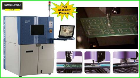
Advanced PCB Assembly
Cutting-edge electronics assembly uses robotic automation and data-driven process control to achieve high precision and reliability.
Surface Mount Technology
Surface mount technology (SMT) has largely replaced through-hole mounting. Smaller SMD (surface mount device) components are soldered directly onto the PCB surface. Fine pitch ball grid arrays and chip scale packages enable higher component densities.
Automated Optical Inspection
AOI (automated optical inspection) systems use high-resolution cameras and machine vision algorithms to detect solder defects, component placement errors, and other flaws. 3D AOI provides even greater accuracy by capturing height information. Automated X-ray inspection is used to verify soldering quality for BGAs and other hidden joints.
Robotic Assembly
Advanced pick-and-place machines can mount thousands of components per hour with great precision. They use high-speed gantries, multiple placement heads, and smart feeders. Flying Probe Testers check circuit functionality by probing test points. Automated conformal coating and potting stations apply protective materials. Robotic soldering handles through-hole components.
Environmental Considerations
As electronic devices proliferate, their environmental impact becomes a major concern. PCB manufacturers are adopting sustainable practices and materials.
Lead-Free Assembly
RoHS (Restriction of Hazardous Substances) regulations have driven the transition to lead-free solders. SAC alloys (Tin/Silver/Copper) have replaced leaded solders in most applications. However, lead-free assembly requires tighter process control due to higher melting points and narrower process windows.
Halogen-Free Laminates
Halogenated flame retardants pose health and environmental risks. Halogen-free PCB Laminates use alternative flame retardants such as metal hydroxides or phosphorus compounds. They reduce toxic gas emissions during firefighting or recycling.
Recycling and Disposal
Proper disposal and recycling of end-of-life electronics is crucial. PCBs contain valuable metals like gold, silver, and copper that can be recovered. However, they also contain hazardous chemicals like lead, cadmium, and brominated flame retardants that must be safely handled. Many countries have implemented e-waste recycling programs and regulations.
Frequently Asked Questions
What is the minimum feature size achievable with HDI PCBs?
HDI PCBs can achieve trace widths and spacing down to 50 microns (2 mil) or less. Microvia diameters can be as small as 50-75 microns. The number of layers in HDI boards can exceed 20.
How do embedded components affect PCB reliability?
Embedding components improves reliability by reducing solder joints and interconnect lengths. However, it also makes rework and repair more challenging. Proper design and process controls are essential to ensure the long-term reliability of embedded component PCBs.
Are 3D printed electronics suitable for high-volume production?
Currently, 3D printed electronics are mainly used for prototyping, low-volume production, and customized devices. The printing process is slower than traditional PCB manufacturing methods. However, advancements in multi-nozzle printers and faster curing processes may enable higher production volumes in the future.
What are the challenges of lead-free soldering?
Lead-free solders have higher melting temperatures, requiring adjustments to the soldering profile. They are also more prone to defects like tin whiskers, brittle fractures, and pad cratering. Careful selection of solder alloys, surface finishes, and process parameters is necessary for reliable lead-free assembly.
How can I ensure my PCB design is environmentally friendly?
To design a green PCB, consider the following:
– Use lead-free and halogen-free materials
– Minimize PCB size to reduce material usage
– Choose components with low standby power
– Facilitate easy disassembly for recycling
– Comply with RoHS and WEEE directives
– Work with environmentally responsible suppliers
Conclusion
Advanced PCB manufacturing is enabling the development of ever-more sophisticated electronic devices. From high-density interconnects and embedded components to 3D printed circuits and eco-friendly materials, PCB technology is continuously evolving. By staying up-to-date with the latest manufacturing capabilities, electronics designers can push the boundaries of performance, miniaturization, and sustainability.
As the world becomes increasingly connected and digitized, advanced PCBs will play a crucial role in realizing the potential of emerging technologies like 5G, IoT, AI, and renewable energy. With ongoing research and innovation in materials science, fabrication processes, and assembly automation, the future of PCB manufacturing looks bright.


Leave a Reply