What is Flying Probe Test?
Flying probe test is an advanced method for testing printed circuit board assemblies (PCBAs) that uses moving test probes to make contact with test points on the board. Unlike traditional bed-of-nails in-circuit test (ICT) fixtures which have fixed probes and require a custom test fixture to be designed for each unique PCBA, flying probe testers have probes that can move to any location on the board. This makes flying probe test much more flexible and enables it to test a wide variety of PCBAs without needing custom hardware.
Flying probe test is well-suited for low to medium volume production and prototypes where the NRE costs of a dedicated ICT fixture would be prohibitive. It is also a good option for PCBAs that are too large or have components that are too tall or tightly spaced for traditional ICT.
How Does Flying Probe Test Work?
A typical flying probe test system has 4 or more moving probes mounted on independent X-Y drive mechanisms that allow them to move horizontally across the board. The probes can also move vertically to make contact with test pads and pins on the top and bottom sides of the PCBA. High resolution cameras help align the probes to test locations.
Here is the basic flying probe test process:
-
The bare PCBA is loaded into the tester either manually or by an automated conveyance system. Typical flying probe testers have a test area of around 20″ x 16″ or larger.
-
Cameras on the tester scan fiducials on the board to determine the board’s exact placement and orientation in the test area. Software aligns the test program to the actual board location.
-
Following the test program, the flying probes move to the first test points and lower to make contact. Each probe can act as either a signal source or measurement sensor.
-
Measurements are made according to the test program. This may include:
- Continuity tests to verify correct connections between nets
- Isolation tests to check for shorts between nets, opens, and missing components
- Analog measurements of resistances, capacitances, diodes, etc.
- Functional tests of ICs by powering them up and communicating over busses like I2C or SPI
-
The probes lift and index to the next set of test points. Steps 3-5 repeat until all tests in the program are completed.
-
The tester reports an overall pass/fail result for the board and provides diagnostic information for any failures found. This data can be logged to a network database.
-
The tested board unloads and the next bare board loads to begin the process again.

Benefits of Flying Probe Test
There are several key advantages that make flying probe test an attractive option vs. ICT:
| Advantage | Description |
|---|---|
| Fast Setup | No custom test fixture required, so test programs can be created quickly |
| Lower NRE Costs | No physical test fixture to design and manufacture |
| Flexible | Can easily handle a variety of board types and sizes |
| Good for Low Volumes | Ideal for prototyping, NPI, and low to medium production volumes |
| Rapid Changeover | Test a different board by simply loading a new program |
| 100% Test Coverage | Can access any location on the PCB top or bottom side |
| Handles Tall Components | No “keep out” areas required for tall parts |
| Handles Fine Pitch | Probes can access tiny pads and fine-pitch leads |
| Automated | Can be integrated into automated manufacturing lines |
These benefits make flying probe test an important tool for electronics manufacturers. The ability to thoroughly test boards without investing in a test fixture allows greater flexibility and faster time to market.

Limitations of Flying Probe Test
While it has many strengths, there are some limitations to flying probe test to be aware of:
| Limitation | Description |
|---|---|
| Slower Than ICT | Moving probes take longer than a simultaneous bed-of-nails test |
| Limited Functional Test | Not well-suited for deep functional testing of the powered-up PCBA |
| Limited Analog Test | Measurements not as precise as dedicated analog ICT instruments |
| Can’t Test Connectors | Probes can’t functionally test connectors |
| Access Issues | May not be able to probe very tight areas or hidden vias |
For simple PCBAs in lower volumes, flying probe is often sufficient as the only electrical test after automated optical inspection (AOI). However, complex and high volume PCBAs typically require ICT and functional circuit test in addition to flying probe.

Flying Probe Test vs. ICT
So how do you decide between flying probe test and ICT? Here are some factors to consider:
| Factor | Flying Probe Test | In-Circuit Test |
|---|---|---|
| Setup Time | Fast, no custom fixturing | Longer, custom fixtures |
| NRE Costs | Low, just need CAD data | Higher, custom fixtures |
| Test Coverage | Good for most faults | Excellent fault coverage |
| Test Speed | Slower, 1-4 mins typical | Faster, <1 min typical |
| Analog Test | Limited | Excellent with guarding |
| Functional Test | Very limited | Good for powered tests |
| Max Board Size | ~20″x16″ typical | Larger fixtures available |
In summary, flying probe test excels in speed and flexibility for prototypes and lower volumes, while ICT provides the best test coverage and speed for higher volumes. The “best” solution is often utilizing both technologies at different stages. Flying probe is used in NPI and early production stages, then an ICT fixture is deployed for mature, higher volume products.
Choosing a Flying Probe Test System
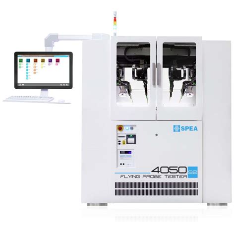
There are several vendors offering flying probe test systems. Some of the most popular include:
- Takaya (Japan)
- ATG Luther & Maelzer (Germany)
- Seica (Italy)
- Circuit Check (USA)
- SPEA (Italy)
- Acculogic (Canada)
When evaluating flying probe test systems, key considerations include:
- Number of probes (4-16)
- Test speed (movements/second)
- Test area (max PCBA size)
- Measurement accuracy and resolution
- Advanced features (contactless testing, boundary scan, etc.)
- Fixturing and board handling options
- Software capabilities and ease of programming
- Price
It’s a good idea to review your PCBA Test requirements and do a side-by-side comparison of each system’s capabilities in relation to your needs and budget.
Best Practices for Flying Probe Test
To get the most out of flying probe test, follow these tips:
-
Involve the test engineer early in the PCBA design process. Small changes to pad and component placement can have a big impact on flying probe access.
-
Provide the flying probe test programmer with detailed documentation including the BOM, schematics, Gerbers, and CAD files. More data allows a more thorough test program to be created.
-
Allow sufficient pad size and space probing. IPC guidelines call for a minimum test pad size of 1.5 mm (0.060″) and spacing of 1.25 mm (0.050″).
-
For repeatable probing of fine-pitch leads and pads, add dedicated test pads connected to the nets you need to probe. This is especially important for QFPs, BGAs, and other tight pitch components.
-
Be aware of test probe keep-out areas under and around tall components. Your contract manufacturer can provide guidance on required clearances.
-
Have a clear test strategy defined that includes coverage requirements, test time goals, and expected yields. This will help guide decisions around flying probe test and complementary ICT and functional test processes.
FAQ
How long does flying probe test take?
Typical flying probe test times range from 1 to 4 minutes per board depending on the board size and complexity and the number of probes on the tester. Compared to an ICT which usually takes less than 1 minute, flying probe test is usually slower because of the need to mechanically move the probes around the board to make contact with the test points one at a time.
Is there a limit to how many test points can be probed?
No, there is no inherent limit to the number test points you can probe with a flying prober. This is one advantage over bed-of-nails ICT where the number of “nails” is limited by the spacing between them on the fixture. With flying probe, you can theoretically test every net on the board one at a time.
Can flying probe test connectors?
Not easily. Since the flying probes are typically simple spring-loaded pogo pins, they can only make electrical contact with exposed test pads or component leads/pins. Testing a connector would require plugging a loopback or some other kind of mating connector into it, which flying probers don’t normally do. Testing connectors is better suited for a custom ICT test fixture or a functional test process.
Is flying probe only for bare board testing?
No, flying probe is commonly used to test fully assembled PCBAs, not just bare PCBs. The main requirement is having test pads or pins accessible by the flying probes. Bare board testing is possible but not common with flying probe since dedicated bare board test systems are optimized for that purpose instead.
How much does a flying prober cost?
Flying probe tester prices range widely from around $75,000 USD to over $300,000 USD depending on the model and options. Compared to an ICT system where a new test fixture must be purchased for each board at a cost of $5,000 to $15,000 each, flying probe has a lower cost of entry since no custom hardware is required. Over time, ICT may have a lower total cost of ownership for high volume products.
I hope this in-depth article provides a solid overview of flying probe test for PCBAs! Let me know if you have any other questions.


Leave a Reply