Introduction to Silkscreen PCB
Printed Circuit Boards (PCBs) are essential components in modern electronics. They provide a platform for mounting and interconnecting electronic components to create functional circuits. One crucial aspect of FlexPCB.org/?p=6507″>PCB Design and manufacturing is the silkscreen layer. Silkscreen, also known as legend or nomenclature, is a printed layer on the PCB that provides important information and aids in the assembly and troubleshooting process.
In this comprehensive article, we will dive deep into the world of silkscreen PCBs. We will explore what silkscreen is, its purpose, the materials and techniques used to apply it, and its significance in the PCB Manufacturing process. By the end of this article, you will have a thorough understanding of silkscreen and its role in creating high-quality and user-friendly PCBs.
What is Silkscreen?
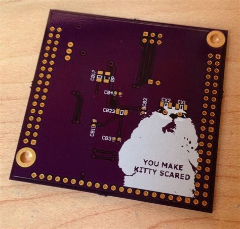
Silkscreen, in the context of PCBs, refers to the layer of text, symbols, and graphics printed on the surface of the PCB. It is typically applied using a screen printing process, where ink is transferred through a fine mesh screen onto the PCB surface. The silkscreen layer is usually white in color, although other colors can be used depending on the specific requirements of the PCB.
The primary purpose of the silkscreen layer is to provide clear and concise information about the components, their placement, and the overall layout of the PCB. It acts as a visual guide for assemblers, technicians, and engineers, making it easier to identify and work with the various components on the board.
Types of Information Included in Silkscreen
The silkscreen layer can include a wide range of information, depending on the complexity and purpose of the PCB. Some common elements found in the silkscreen layer include:
- Component designators: These are the unique identifiers for each component on the PCB, such as R1 for a resistor or C2 for a capacitor.
- Component values: The silkscreen may include the values of certain components, such as the resistance value of a resistor or the capacitance of a capacitor.
- Polarity indicators: For components with specific polarity requirements, such as electrolytic capacitors or diodes, the silkscreen may include polarity markers (+ or -) to ensure correct orientation during assembly.
- Test points: The silkscreen may designate test points on the PCB, which are used for testing and debugging purposes.
- Company logos and branding: The silkscreen layer can include company logos, product names, or other branding elements to enhance the visual appeal and brand recognition of the PCB.
- Warning symbols: In some cases, the silkscreen may include warning symbols or text to indicate areas of the PCB that require special handling or caution.
Silkscreen Materials and Techniques
The silkscreen layer is typically applied using a screen printing process. This involves creating a fine mesh screen with the desired silkscreen artwork. The artwork is created as a negative image, where the areas to be printed are left open, and the rest of the screen is blocked off.
The screen is then placed over the PCB, and ink is applied to the screen using a squeegee. The ink passes through the open areas of the screen and onto the PCB surface, creating the silkscreen layer. The ink used for silkscreen printing is specially formulated to adhere to the PCB surface and withstand the various manufacturing processes and environmental conditions that the PCB may encounter.
The most common material used for silkscreen ink is epoxy-based ink. This type of ink is known for its durability, resistance to chemicals and solvents, and excellent adhesion to the PCB surface. Other types of inks, such as UV-curable or solvent-based inks, may also be used depending on the specific requirements of the PCB.

Importance of Silkscreen in PCB Manufacturing
The silkscreen layer plays a crucial role in the PCB manufacturing process and the overall functionality and usability of the final product. Let’s explore some of the key reasons why silkscreen is so important:
1. Assembly and Manufacturing
During the PCB Assembly process, the silkscreen layer acts as a visual guide for the assembly technicians. The component designators and polarity indicators printed on the silkscreen help ensure that the correct components are placed in the right locations and with the proper orientation. This reduces the risk of assembly errors and improves the overall quality and reliability of the PCB.
In addition to aiding in the assembly process, the silkscreen layer also helps during the manufacturing process. The silkscreen can include fiducial markers, which are used as reference points for automated assembly equipment. These markers help align the PCB correctly and ensure precise component placement.
2. Troubleshooting and Repair
In the event that a PCB malfunctions or requires repair, the silkscreen layer becomes an invaluable tool for technicians and engineers. The component designators and test points printed on the silkscreen allow technicians to quickly identify and locate specific components or areas of the PCB that may be causing issues. This can significantly reduce the time and effort required to diagnose and repair the PCB, ultimately saving time and money.
3. User Interface and Aesthetics
The silkscreen layer also plays a role in the user interface and overall aesthetics of the PCB. In some cases, the silkscreen may include labels or instructions that help users interact with the PCB or the device it is a part of. For example, a silkscreen label near a button or switch can indicate its function, making it easier for users to operate the device.
Additionally, the silkscreen layer can enhance the visual appeal of the PCB. Company logos, product names, or other branding elements can be incorporated into the silkscreen design to create a professional and polished look. This can be particularly important for consumer-facing products where aesthetics play a significant role in the overall user experience.

Best Practices for Silkscreen Design
To ensure that the silkscreen layer on your PCB is effective and of high quality, there are several best practices to keep in mind during the design process:
1. Legibility
The primary purpose of the silkscreen is to provide clear and easily readable information. When designing the silkscreen artwork, ensure that the text and symbols are large enough to be easily read by the human eye. A minimum text height of 0.8mm is generally recommended, although larger text may be necessary for certain applications.
2. Placement
When placing silkscreen elements on the PCB, consider the location of components and other features to avoid interference or obstruction. Ensure that the silkscreen does not overlap with component pads, vias, or other critical areas of the PCB. Additionally, maintain a minimum clearance between the silkscreen and the edge of the PCB to prevent the silkscreen from being cut off during the manufacturing process.
3. Contrast
To enhance the readability of the silkscreen, ensure that there is sufficient contrast between the silkscreen ink and the PCB surface. White silkscreen ink on a dark PCB surface, or black ink on a light surface, provides the best contrast and legibility.
4. Consistency
Maintain consistency in the silkscreen design across the entire PCB. Use the same font, text size, and formatting for all similar elements, such as component designators or test points. This helps create a cohesive and professional appearance and makes it easier for technicians and engineers to navigate the PCB.
5. Simplicity
While it may be tempting to include a lot of information in the silkscreen layer, it is important to strike a balance between providing necessary information and maintaining simplicity. Too much clutter on the silkscreen can make it difficult to read and interpret. Focus on including the most essential information and avoid unnecessary or redundant elements.

Frequently Asked Questions (FAQ)
1. Is silkscreen necessary on every PCB?
While silkscreen is highly recommended for most PCBs, it may not be strictly necessary for every application. In some cases, such as very simple PCBs or those with limited space, the silkscreen layer may be omitted. However, for the majority of PCBs, especially those with multiple components or those that will be assembled or serviced by technicians, the silkscreen layer is considered essential.
2. Can silkscreen be applied to both sides of the PCB?
Yes, silkscreen can be applied to both the top and bottom sides of the PCB. In fact, it is common for PCBs to have silkscreen on both sides to provide information about components and layout on each side of the board.
3. What is the minimum text size for silkscreen?
The minimum recommended text height for silkscreen is 0.8mm. However, larger text may be necessary for certain applications or to ensure better readability. It is important to consider the viewing distance and the environment in which the PCB will be used when determining the appropriate text size.
4. Can silkscreen be applied in colors other than white?
While white is the most common color for silkscreen ink, other colors can be used depending on the specific requirements of the PCB. Some common alternative colors include black, yellow, and red. The choice of color should be based on factors such as the color of the PCB surface, the desired contrast and readability, and any aesthetic considerations.
5. How durable is the silkscreen layer?
The durability of the silkscreen layer depends on several factors, including the type of ink used, the PCB material, and the environmental conditions to which the PCB will be exposed. Epoxy-based inks, which are the most commonly used for silkscreen, offer excellent durability and resistance to chemicals, solvents, and abrasion. When properly applied and cured, the silkscreen layer can withstand the rigors of the PCB manufacturing process and provide long-lasting legibility and functionality.
Conclusion
Silkscreen is a vital component of PCB design and manufacturing, providing essential information and enhancing the overall functionality and usability of the PCB. By understanding the purpose, materials, and best practices associated with silkscreen, PCB designers and manufacturers can create high-quality and user-friendly PCBs that meet the needs of their intended applications.
From aiding in the assembly process to facilitating troubleshooting and repair, the silkscreen layer plays a crucial role in the lifecycle of a PCB. By following best practices such as ensuring legibility, proper placement, sufficient contrast, consistency, and simplicity, designers can create silkscreen artwork that effectively communicates necessary information and enhances the overall quality of the PCB.
As PCB Technology continues to evolve, the importance of silkscreen remains constant. By staying up-to-date with the latest techniques and materials related to silkscreen PCBs, designers and manufacturers can continue to create innovative and reliable electronic devices that meet the ever-growing demands of the industry.


Leave a Reply