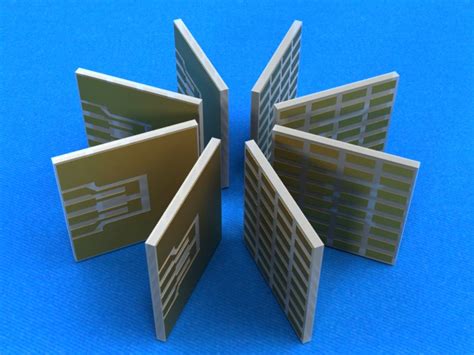
Introduction to Ceramic PCBs
Ceramic printed circuit boards (PCBs) are a specialized type of PCB that uses ceramic materials as the substrate instead of the more common FR-4 or other organic materials. Ceramic PCBs offer unique properties that make them ideal for certain applications, particularly those involving high temperatures, high frequencies, or extreme environments.
Advantages of Ceramic PCBs
Ceramic PCBs offer several advantages over traditional PCBs:
- High thermal conductivity
- Low dielectric constant
- High mechanical strength
- Excellent dimensional stability
- Resistance to harsh environments
These properties make ceramic PCBs well-suited for applications in aerospace, military, and high-power electronics.
Materials Used in Ceramic PCBs
CeramIC Substrates
The most common ceramic materials used in PCBs are:
- Alumina (Al2O3)
- Aluminum Nitride (AlN)
- Beryllium Oxide (BeO)
Each material has its own unique properties, as shown in the table below:
| Material | Thermal Conductivity (W/mK) | Dielectric Constant | Mechanical Strength (MPa) |
|---|---|---|---|
| Alumina | 20-30 | 9.8 | 300-500 |
| AlN | 150-180 | 8.8 | 300-400 |
| BeO | 260-300 | 6.7 | 200-300 |
Conductive Materials
Conductive materials used in ceramic PCBs include:
- Copper
- Silver
- Gold
These materials are used for creating conductive traces, pads, and vias on the ceramic substrate.
 DRCYI9P5UAdMlPmCuwJwMcgZPT8ce1MBrEZOcktu45zycjn19+340oBChiN6bvmDNtwzDgA9c+/SgBSwGcAnrJ8gB5PzbeM+tOVVkMeSqfdTeFZvmI+ZiPX2oARV2h3UAqh2sHHzAnjaR0/p/KmkMO/wDskn0BDFOe3t/jQ7OcZCh1Xa+3JDBeD06j1/8ArUu0Pv6hV3btu5+gAAB7j09KoQKzYcqq4KsNjYf5DyThv8im7sZHXdh2wTxtA4JH5A+/5KwDeYRGowq8R4AXHyhgAep9fXJpAMZPAIycnuxOMEf5Bx70CHMQqkZPOD8uMDHQHH/6j+NDbWLIg+UM3CgjA2g8H29OlNUuAWQkPISoAAOFfJ78A+oP4dadG20bg4Hl7cfxbi2eMcfj9aYxqtgHH32X5SDjaGwCCMf5/mu8AbB93LHoMkDg/MvP+FBDMOQFOzcp253Ad3HcfqKbjBweCcFsncuNuMsR296BDsbiAMKOgY9SM8s2Ofxx2poJLDOAOpPQ+pLH1p33FKggEYJx1UDgDcPcknt/RAeWIwAMjAIHfHy56f1qhNgztkheFGMKenOWIw3fuaevPlsMkhcYO3A6nAB5P0pEAcsOQu3DBc4VS4UnHOfp/hSNyflxtJYKFzyue2M9KaEKQHZiWXgNhjllYgdMU0rkAgN93ezE42g4AwR26c0uT8keVOXyrAn5iw6NinA7k6KFQhmXPJJGcrgZz+lMQhJAJZU2yqxAI6EEDeAOPpTdqf3v0/8Ar1IFVwrMQwJ+VUIRhwOgHTr0pdif7H/fs/40IGZUi7ehycE5POcHoaacEEgY4Gec5z60UVktikOVdzbCT95Vz04PfHrSEkjr91wmBxye9FFIYINzBc8ZcceoUnP09qMcqCc54Ge2O2PSiiqJEHIJ7BGbHXo4GKdnYBIM5DA4zwc8ciiimA4rtBYE7l2EHvznFJnaT33ttPbkj7w/rRRSsNC4KsQCMh9gOOmVLZA6fUU4YbnGOJDx7cn8KKKkYDJHHy/IW9eBxtOf0oXJXd6AEfT0z/WiigBwB+RwSHBXDDryQM5p7BSiEgf6x43xxuYH7/HeiigBijcSp9Sgx2bru/8ArUigEqexGCDz90Z6+lFFJjRJGwLISCV27ypJ5UKTtLDn6HNI+AZOp2ZI6dxnrjr70UUDHN8rbMk4ZiOcYOAcgClwA2BwVcxgjHByAWAPHOeRRRQBIgAWOReGZpoR3UBGKkYPY9xTyqrEMAfvEjl5ySASw2kk+2aKKljI1wSmd2B5BwDg7XOCAT398VLKAmF4xHN5S7eDlt2XJOee9FFAxFT541YkiR2X5flIOzOQefypiZ4OSCd+3bkBQFBwASeOcf8A66KKYhVxJ8pGPkkYnqTtOMc9v85oyzbixyWjMjZ6lRgbQevfg/40UUEjx1kZyWIw3Hyklj9444z+FIoYsx3c+cI+Rn5jk7vX6jPNFFBSFgTfNAM4LHGT8wzkjkHqPUe/5OQG4kjLHaZEd+Bwvlox2genHHp+FFFABuLeeTncFQoxJ+QK7R4Hvx196jJBDAg/KSMg46AAEehHrRRQA75YpFicb037SM7eWO3dxTNvCHPWR0HfaVIJxnsfSiimIdGpbbyMOHGMcDbk9uo9PSnFj8yklo7dA6I+DwT93Ix+BoopgIFwxOeRsIOMEEnAOfUdaQjaXH9xgpPdieAaKKAHhAVRMKPMdyWxkgAY2jJ6d6WdDE6oXLBoYpxkAbSUHH4djRRQBGRhGI+8FEhbnJ3EcdevbNSSr5agAk/vAepA+ZQ3Qd+cf0ooqhDOmMAfIVznJUnaWJ2k456H/wCvQkXmbBuAyJGPHGY03jgEcdqKKBDWyyI5YlnG0FiSVVF+7n0/wpD82Fwu1IiRxyQrIuCR9etFFUAHq5yeM9TzlmxnPrUkKhvPXo8bxSI4xkb2Ixj8KKKQmMiG/PYqQuR1xz0/L9aAm/ac4J8wdMj5Bv59u1FFUSwBynRchQxPOSEX5VGD25xSBiFZz8xDAfNyQNueDRRTAUjaFx97ZkH0BHTFDBVkKY4V2jOOMn1/TpRRTAeWKDA4CvtO3gkk4yCc/wCe9KISQD5j8gHt3oorObaWhUUnuf/Z” alt=”” class=”wp-image-136″ >
Manufacturing Process of Ceramic PCBs
The manufacturing process of ceramic PCBs involves several steps:
- Substrate preparation
- Metallization
- Patterning
- Firing
- Assembly
Substrate Preparation
The ceramic substrate is prepared by mixing ceramic powders with binders and pressing them into the desired shape. The substrate is then sintered at high temperatures to create a solid, dense material.
Metallization
Conductive materials are applied to the ceramic substrate using various methods, such as screen printing, sputtering, or plating. The most common method is screen printing, which involves applying a conductive paste through a patterned screen onto the substrate.
Patterning
The conductive layer is patterned using photolithography or laser etching to create the desired circuit layout.
Firing
After patterning, the ceramic PCB is fired at high temperatures (typically 850-1000°C) to sinter the conductive materials and create a strong bond with the substrate.
Assembly
Finally, components are assembled onto the ceramic PCB using various techniques, such as Wire Bonding, flip-chip bonding, or surface mount technology (SMT).

Applications of Ceramic PCBs
Ceramic PCBs find applications in various industries, including:
- Aerospace
- Military
- Automotive
- Medical
- High-power electronics
Some specific applications include:
- Satellite communications
- Radar systems
- Engine control units
- Implantable medical devices
- Power modules

Advantages and Disadvantages of Ceramic PCBs
Advantages
- High thermal conductivity enables efficient heat dissipation
- Low dielectric constant allows for high-frequency operation
- High mechanical strength provides durability in harsh environments
- Excellent dimensional stability ensures consistent performance over a wide temperature range
- Resistance to chemicals, moisture, and radiation
Disadvantages
- Higher cost compared to traditional PCBs
- Limited design flexibility due to the brittle nature of ceramics
- Requires specialized manufacturing processes and equipment
- Limited availability of materials and suppliers
Future Trends in Ceramic PCBs
As technology advances, the demand for ceramic PCBs is expected to grow in various industries. Some future trends in ceramic PCBs include:
- Development of new ceramic materials with improved properties
- Advancements in manufacturing processes to reduce costs and improve efficiency
- Increased adoption in 5G and millimeter-wave applications
- Integration of ceramic PCBs with other technologies, such as microfluidics and sensors
Frequently Asked Questions (FAQs)
1. What is the difference between ceramic and traditional PCBs?
Ceramic PCBs use ceramic materials as the substrate, while traditional PCBs use organic materials like FR-4. Ceramic PCBs offer higher thermal conductivity, lower dielectric constant, and better mechanical strength compared to traditional PCBs.
2. What are the most common ceramic materials used in PCBs?
The most common ceramic materials used in PCBs are alumina (Al2O3), aluminum nitride (AlN), and beryllium oxide (BeO).
3. What are the main advantages of using ceramic PCBs?
The main advantages of using ceramic PCBs include high thermal conductivity, low dielectric constant, high mechanical strength, excellent dimensional stability, and resistance to harsh environments.
4. In which industries are ceramic PCBs commonly used?
Ceramic PCBs are commonly used in industries such as aerospace, military, automotive, medical, and high-power electronics.
5. Are ceramic PCBs more expensive than traditional PCBs?
Yes, ceramic PCBs are generally more expensive than traditional PCBs due to the specialized materials and manufacturing processes required.
Conclusion
Ceramic PCBs are a specialized type of printed circuit board that offer unique properties, making them ideal for applications that require high thermal conductivity, low dielectric constant, and resistance to harsh environments. While they may be more expensive than traditional PCBs, ceramic PCBs play a crucial role in various industries, including aerospace, military, and high-power electronics.
As technology continues to advance, the demand for ceramic PCBs is expected to grow, driven by the development of new materials, manufacturing processes, and applications. By understanding the advantages, manufacturing process, and applications of ceramic PCBs, engineers and designers can make informed decisions when selecting the most appropriate PCB technology for their projects.


Leave a Reply