Introduction to Wire Bonding
Wire bonding is a widely used interconnection technology in the semiconductor packaging industry. It is a process that involves connecting the chip’s bond pads to the package leadframe or substrate using thin metal wires, typically made of gold, aluminum, or copper. Wire bonding has been a reliable and cost-effective method for creating electrical connections between the integrated circuit (IC) and the package for several decades.
Advantages of Wire Bonding
Wire bonding offers several advantages over other interconnection technologies:
- Cost-effectiveness: Wire bonding is an economical process compared to other interconnection methods, making it suitable for high-volume production.
- Flexibility: Wire bonding can be used with a variety of chip and package types, allowing for design flexibility.
- Reliability: When properly executed, wire bonds provide reliable electrical connections that can withstand various environmental conditions.
- Adaptability: Wire bonding equipment can be easily adapted to accommodate changes in chip and package designs.
Wire Bonding Process
The wire bonding process typically involves the following steps:
1. Die Attachment
The first step is to attach the semiconductor die to the package substrate or leadframe using an adhesive, such as epoxy or solder. This process ensures that the die is securely fixed to the package and provides a stable base for wire bonding.
2. Wire Bonding
Once the die is attached, the wire bonding process begins. There are two primary wire bonding techniques:
a. Ball Bonding
Ball bonding is the most common wire bonding method. It involves the following steps:
- A thin wire, usually gold, is threaded through a capillary tool.
- A high-voltage electric flame-off (EFO) melts the wire tip, forming a ball.
- The capillary tool descends and presses the ball against the bond pad on the chip, creating the first bond.
- The capillary tool then moves to the package leadframe or substrate, forming a loop and creating the second bond.
- The wire is then cut, and the process is repeated for the next bond.
b. Wedge Bonding
Wedge bonding, also known as ultrasonic bonding, is another wire bonding technique. It involves the following steps:
- A thin wire, usually aluminum or gold, is threaded through a wedge-shaped tool.
- The wedge tool descends and presses the wire against the bond pad on the chip, creating the first bond using ultrasonic energy and pressure.
- The wedge tool then moves to the package leadframe or substrate, forming a loop and creating the second bond using the same method.
- The wire is then cut, and the process is repeated for the next bond.
3. Encapsulation
After wire bonding, the package undergoes an encapsulation process to protect the chip and the wire bonds from environmental factors such as moisture, contamination, and mechanical stress. The most common encapsulation methods are transfer molding and glob top encapsulation.

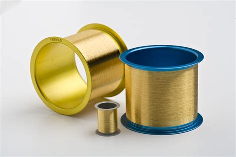
Wire Bonding Materials
The choice of wire material depends on several factors, including the chip and package type, the desired electrical and mechanical properties, and the cost. The most common wire materials used in wire bonding are:
- Gold (Au): Gold is the most widely used wire material due to its excellent electrical conductivity, corrosion resistance, and bond reliability. However, it is also the most expensive option.
- Aluminum (Al): Aluminum is a popular choice for wedge bonding due to its lower cost and good electrical conductivity. It is often used in power devices and high-frequency applications.
- Copper (Cu): Copper wire bonding has gained popularity in recent years due to its lower cost compared to gold and better electrical and thermal conductivity than aluminum. However, copper wire bonding requires a more complex process and higher bonding forces.
The following table compares the properties of these common wire bonding materials:
| Property | Gold (Au) | Aluminum (Al) | Copper (Cu) |
|---|---|---|---|
| Electrical Conductivity | High | Moderate | High |
| Thermal Conductivity | Moderate | High | High |
| Corrosion Resistance | Excellent | Good | Moderate |
| Ease of Bonding | Easy | Moderate | Difficult |
| Cost | High | Low | Moderate |

Challenges and Advancements in Wire Bonding
As the semiconductor industry continues to evolve, wire bonding faces several challenges and opportunities for improvement:
1. Finer Pitch and Smaller Chip Sizes
With the trend towards miniaturization, chips are becoming smaller, and bond pad pitches are decreasing. This requires the development of finer pitch wire bonding techniques and equipment to ensure reliable connections.
2. Increased Number of I/Os
As the complexity of ICs increases, the number of input/output (I/O) connections also rises. This demands higher throughput wire bonding processes and equipment to maintain cost-effectiveness and production efficiency.
3. Advanced Packaging Technologies
The emergence of advanced packaging technologies, such as 2.5D and 3D packaging, presents new challenges for wire bonding. These technologies often require the integration of wire bonding with other interconnection methods, such as through-silicon vias (TSVs) and flip-chip bonding.
To address these challenges, wire bonding technology continues to evolve:
- Automated wire bonding machines: Modern wire bonding equipment incorporates advanced automation features, such as pattern recognition and real-time process monitoring, to improve yield and throughput.
- Multi-layer wire bonding: This technique involves stacking wire bonds on top of each other to increase interconnection density and reduce package size.
- Insulated wire bonding: By using insulated wires, such as those coated with polymers, wire bonds can be placed closer together without the risk of short-circuiting, enabling finer pitch bonding.
- Copper wire bonding: As mentioned earlier, copper wire bonding is gaining popularity due to its cost and performance benefits. Advancements in copper wire bonding processes and equipment are making it a more viable option for a wider range of applications.

Future of Wire Bonding
Despite the challenges, wire bonding remains a critical interconnection technology in the semiconductor packaging industry. Its adaptability, cost-effectiveness, and reliability ensure that it will continue to play a significant role in the foreseeable future. As the industry advances, wire bonding technology will likely co-exist and integrate with other interconnection methods to meet the ever-increasing demands for performance, functionality, and miniaturization in semiconductor packages.
Frequently Asked Questions (FAQ)
-
Q: What is wire bonding, and why is it important in semiconductor packaging?
A: Wire bonding is a process that involves connecting the semiconductor chip’s bond pads to the package leadframe or substrate using thin metal wires. It is important because it provides reliable and cost-effective electrical connections between the chip and the package, enabling the chip to communicate with the outside world. -
Q: What are the most common wire materials used in wire bonding?
A: The most common wire materials used in wire bonding are gold (Au), aluminum (Al), and copper (Cu). Gold is widely used for its excellent electrical conductivity and reliability, while aluminum is preferred for wedge bonding and copper is gaining popularity due to its cost and performance benefits. -
Q: What are the two main wire bonding techniques?
A: The two main wire bonding techniques are ball bonding and wedge bonding. Ball bonding involves creating a ball at the end of the wire using an electric flame-off (EFO) and pressing it against the bond pad, while wedge bonding uses a wedge-shaped tool to press the wire against the bond pad using ultrasonic energy and pressure. -
Q: How does wire bonding adapt to the trend of miniaturization in the semiconductor industry?
A: As chips become smaller and bond pad pitches decrease, wire bonding technology is evolving to accommodate these changes. Advancements such as finer pitch wire bonding techniques, multi-layer wire bonding, insulated wire bonding, and automated wire bonding machines help address the challenges posed by miniaturization. -
Q: Will wire bonding become obsolete with the emergence of advanced packaging technologies?
A: While advanced packaging technologies, such as 2.5D and 3D packaging, present new challenges for wire bonding, it is unlikely that wire bonding will become obsolete in the near future. Instead, wire bonding is expected to co-exist and integrate with other interconnection methods to meet the diverse requirements of the semiconductor industry.
In conclusion, wire bonding remains a vital interconnection technology in the semiconductor packaging industry, offering a cost-effective, reliable, and flexible solution for creating electrical connections between chips and packages. As the industry continues to evolve, wire bonding technology will adapt and integrate with other methods to meet the ever-increasing demands for performance, functionality, and miniaturization in semiconductor packages.


Leave a Reply