Introduction to Buried vias
A buried via is a type of interconnect used in multi-layer printed circuit boards (PCBs) to electrically connect two or more inner layers without being visible on the top or bottom outer layers of the board. Buried vias are “buried” in the inner layers of the PCB, unlike through-hole vias that go through all layers and are exposed on the top and bottom surfaces.
Key Characteristics of Buried Vias
- Connect inner layers only, not visible on outer layers
- Drilled and plated only where needed
- Enable higher density routing on outer layers
- Typically used on PCBs with 4 or more layers
- More expensive than through-hole vias
- Require additional manufacturing steps
Advantages of Using Buried Vias
Increased Routing Density
One of the main advantages of using buried vias in a PCB design is the ability to increase the routing density on the outer layers of the board. By freeing up space that would otherwise be occupied by through-hole via pads, a higher density of signal traces can be routed on the top and bottom layers.
This is especially beneficial in designs with complex, high-density routing requirements, such as:
- High-speed digital circuits
- RF and microwave designs
- Miniaturized devices with limited PCB real estate
Improved Signal Integrity
Buried vias can also contribute to improved signal integrity in a PCB design. By providing more direct connections between inner layers, signal paths can be kept shorter and potentially reduce issues such as:
- Crosstalk
- Electromagnetic interference (EMI)
- Signal reflections
Additionally, the absence of via stubs (unused portions of through-hole vias) can help minimize unwanted signal reflections and improve overall signal quality.
Enhanced Mechanical Strength
Since buried vias do not extend through the entire thickness of the PCB, they can contribute to enhanced mechanical strength compared to through-hole vias. This is particularly relevant in applications where the PCB may be subjected to physical stress, vibration, or shock.
The increased mechanical integrity provided by buried vias can help prevent issues such as:
- Via barrel cracking
- Pad lifting
- Delamination of PCB Layers

Disadvantages of Using Buried Vias
Increased Manufacturing Complexity
One of the main drawbacks of using buried vias is the increased manufacturing complexity involved. Unlike through-hole vias, which can be drilled and plated in a single process, buried vias require additional steps:
- Drilling and plating the buried vias on the relevant inner layers
- Laminating the inner layers together
- Drilling and plating the through-hole vias (if any)
This multi-step process can increase the overall manufacturing time and cost compared to PCBs using only through-hole vias.
Higher Production Costs
As a result of the increased manufacturing complexity, PCBs with buried vias generally have higher production costs than those using only through-hole vias. The additional processing steps, material usage, and time required contribute to the increased expense.
However, the cost premium for buried vias has decreased over time as manufacturing processes have improved and become more standardized. In many cases, the benefits of using buried vias can outweigh the added cost, particularly in high-density, high-performance applications.
Potential Reliability Concerns
While buried vias offer several advantages, there are also some potential reliability concerns to consider:
- Increased risk of manufacturing defects due to the additional processing steps
- Potential for weak points or voids in the Via Plating, leading to electrical or mechanical failures
- Difficulty in inspecting and testing buried vias compared to through-hole vias
To mitigate these concerns, it is essential to work with a reputable PCB manufacturer with experience in producing boards with buried vias and to adhere to industry standards and best practices for design and manufacturing.

Applications of Buried Vias
Buried vias find use in a wide range of electronics applications where high density, signal integrity, and mechanical robustness are important. Some common applications include:
High-Speed Digital Devices
- Smartphones and tablets
- Laptops and desktop computers
- Gaming consoles
- Wearable electronics
RF and Microwave Circuits
- Wireless communication devices (e.g., cell phones, Wi-Fi routers)
- Radar and satellite systems
- High-frequency test and measurement equipment
Medical Electronics
- Implantable devices (e.g., pacemakers, neurostimulators)
- Portable medical monitors and diagnostic tools
- Imaging equipment (e.g., ultrasound, X-ray)
Aerospace and Defense Systems
- Avionics and flight control systems
- Military communications equipment
- Satellite and space hardware
Automotive Electronics
- Engine control units (ECUs)
- Advanced driver assistance systems (ADAS)
- Infotainment and navigation systems

Design Considerations for Buried Vias
When incorporating buried vias into a PCB design, several key factors must be considered to ensure optimal performance, reliability, and manufacturability:
Via Size and Spacing
- Minimum via diameter and drill size
- Annular Ring size (pad to hole clearance)
- Via-to-via spacing
- Via-to-trace spacing
These parameters are typically dictated by the PCB manufacturer’s capabilities and the specific design requirements.
Stack-Up Planning
- Number and arrangement of layers
- Dielectric material properties
- Copper thickness and weight
- Symmetry and balance of the stack-up
Careful planning of the PCB Stack-Up is crucial to ensure proper Impedance Control, signal integrity, and mechanical stability.
Routing and Placement
- Signal trace routing and length matching
- Component placement and orientation
- Ground and power plane design
- Thermal management considerations
Optimal routing and placement strategies can help maximize the benefits of using buried vias while minimizing potential issues.
Manufacturing Tolerances
- Drill size and position accuracy
- Plating thickness and uniformity
- Layer registration and alignment
- Copper etching and solder mask tolerances
Understanding and accounting for manufacturing tolerances is essential to ensure the designed buried vias can be reliably produced and function as intended.
Manufacturing Process for Buried Vias
The manufacturing process for PCBs with buried vias involves several key steps:
-
Inner Layer Processing: The inner layers containing the buried vias are patterned, etched, and plated according to the design specifications.
-
Lamination: The inner layers are stacked and laminated together under heat and pressure to form a solid, multi-layer structure.
-
Drilling: Through-holes (if any) are drilled through the entire PCB stack-up.
-
Plating: The through-holes and any remaining exposed buried vias are plated with copper to establish electrical connectivity.
-
Outer Layer Processing: The outer layers are patterned, etched, and plated, similar to the inner layer processing.
-
Solder Mask and Silkscreen: A protective solder mask is applied to the outer layers, and silkscreen legends are printed for component identification and assembly.
-
Surface Finish: The exposed copper areas (pads and vias) are coated with a surface finish (e.g., HASL, ENIG, or OSP) to protect against oxidation and facilitate soldering.
-
Electrical Testing: The completed PCB undergoes electrical testing to verify connectivity, isolation, and performance.
-
Singulation: The individual PCBs are cut out from the manufacturing panel.
FAQ
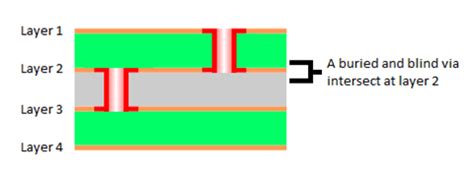
1. What is the difference between a buried via and a blind via?
A buried via connects two or more inner layers of a PCB without being visible on the top or bottom surfaces. A blind via, on the other hand, connects an inner layer to either the top or bottom surface, but not both. Blind vias are visible on one of the outer layers.
2. Can buried vias be used in any PCB design?
Buried vias are typically used in PCBs with four or more layers due to the need for inner layer connections. They may not be necessary or cost-effective for simpler, double-layer designs. The decision to use buried vias depends on the specific requirements of the circuit, such as routing density, signal integrity, and mechanical constraints.
3. How much more expensive are PCBs with buried vias compared to those without?
The cost premium for PCBs with buried vias can vary depending on factors such as the number of layers, the complexity of the design, and the manufacturing process. In general, buried vias can increase the cost of a PCB by 20-50% compared to a similar design without buried vias. However, the exact cost difference will depend on the specific project and the PCB manufacturer.
4. Are there any limitations on the number or placement of buried vias in a PCB?
The number and placement of buried vias in a PCB are primarily limited by the manufacturing capabilities of the PCB fabricator and the design rules for the specific project. Factors such as minimum via size, spacing, and aspect ratio (depth to diameter) can restrict the density and location of buried vias. It is essential to consult with the PCB manufacturer early in the design process to ensure the proposed use of buried vias is feasible and cost-effective.
5. Can buried vias be repaired or reworked if they fail?
Repairing or reworking buried vias can be challenging, if not impossible, due to their internal location within the PCB. In most cases, a failure of a buried via will require the replacement of the entire PCB. This underscores the importance of proper design, manufacturing, and testing to ensure the reliability of buried vias in the final product.
Conclusion
Buried vias are an essential interconnect technology for modern, high-density PCBs. By providing electrical connections between inner layers without consuming space on the outer surfaces, buried vias enable increased routing density, improved signal integrity, and enhanced mechanical strength.
However, the use of buried vias also comes with trade-offs, such as increased manufacturing complexity, higher production costs, and potential reliability concerns. Careful consideration of design requirements, manufacturing capabilities, and cost constraints is necessary when deciding whether to incorporate buried vias into a PCB design.
As electronics continue to push the boundaries of performance and miniaturization, the use of buried vias will likely remain a key strategy for achieving the demanding requirements of advanced applications. By understanding the benefits, limitations, and best practices associated with buried vias, PCB designers and manufacturers can effectively leverage this technology to create innovative, reliable, and cost-effective electronic products.


Leave a Reply