Introduction to Transparent PCBs
Transparent PCBs, also known as clear or glass PCBs, are a revolutionary development in the world of printed circuit boards. Unlike traditional PCBs that are made from opaque materials like FR-4, transparent PCBs are fabricated using clear substrates such as glass or flexible polymers. This unique property allows for a wide range of applications and benefits, including enhanced aesthetics, improved visibility, and increased design flexibility.
In this comprehensive article, we will explore the world of transparent PCBs, delving into their types, manufacturing processes, advantages, and potential applications. We will also address some frequently asked questions to provide a thorough understanding of this innovative technology.
Types of Transparent PCBs
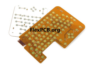
Clear Flexible PCBs
Clear flexible PCBs are manufactured using transparent polymeric materials, such as polyethylene terephthalate (PET) or polyimide (PI). These materials offer excellent flexibility, allowing the PCBs to be bent, twisted, or folded without damaging the circuits. Clear flexible PCBs are ideal for applications that require conformity to irregular shapes or where space is limited.
Key characteristics of clear flexible PCBs include:
– High flexibility and durability
– Lightweight and thin profile
– Excellent electrical insulation properties
– Resistance to moisture and chemicals
– Suitable for dynamic and high-stress environments
Glass PCBs
Glass PCBs are fabricated using a transparent glass substrate, typically borosilicate or soda-lime glass. These PCBs offer superior dimensional stability, high thermal resistance, and excellent electrical insulation properties. Glass PCBs are often used in applications that require high transparency, such as displays, lighting, and optical sensors.
Key characteristics of glass PCBs include:
– Excellent transparency and optical clarity
– High thermal resistance and dimensional stability
– Superior electrical insulation properties
– Resistance to moisture, chemicals, and UV radiation
– Suitable for high-frequency and high-temperature applications
Manufacturing Process of Transparent PCBs
The manufacturing process of transparent PCBs differs from that of traditional PCBs due to the unique properties of the clear substrates. Here’s an overview of the key steps involved in fabricating transparent PCBs:
- Substrate Preparation: The clear substrate, either flexible polymer or glass, is cleaned and treated to ensure proper adhesion of the conductive traces.
- Copper Deposition: A thin layer of copper is deposited onto the substrate using techniques such as sputtering, electroless plating, or lamination.
- Patterning: The desired circuit pattern is created on the copper layer using photolithography or laser direct imaging (LDI).
- Etching: The unwanted copper is removed using chemical etching, leaving only the desired conductive traces.
- Protective Coating: A clear protective layer, such as solder mask or coverlay, is applied to protect the circuits and improve the PCB’s durability.
- Surface Finish: Optional surface finishes, such as immersion gold or ENIG (Electroless Nickel Immersion Gold), can be applied to enhance the PCB’s solderability and corrosion resistance.
- Cutting and Drilling: The PCB panel is cut into individual boards, and any necessary holes or slots are drilled.
- Inspection and Testing: The finished transparent PCBs undergo rigorous quality control inspections and electrical testing to ensure functionality and reliability.

Advantages of Transparent PCBs
Transparent PCBs offer several unique advantages over traditional opaque PCBs, making them an attractive choice for various applications:
- Enhanced Aesthetics: The clear substrate allows for visually appealing designs, enabling the creation of unique and eye-catching products.
- Improved Visibility: Transparent PCBs allow for easy inspection of the underlying components and circuits, facilitating troubleshooting and quality control.
- Increased Design Flexibility: Clear substrates enable the integration of PCBs with displays, sensors, or other optical components, opening up new design possibilities.
- Lightweight and Thin Profile: Transparent PCBs, particularly clear flexible PCBs, are typically thinner and lighter than traditional PCBs, making them suitable for portable and wearable devices.
- Superior Electrical Properties: Glass PCBs offer excellent electrical insulation and low dielectric constant, making them ideal for high-frequency applications.
- Environmental Resistance: Transparent PCBs can be designed to withstand harsh environments, including exposure to moisture, chemicals, and extreme temperatures.

Applications of Transparent PCBs
Transparent PCBs find applications in various industries and products, leveraging their unique properties and advantages. Some notable applications include:
- Consumer Electronics: Transparent PCBs are used in smartphones, tablets, and wearable devices to enable touch sensors, displays, and NFC Antennas.
- Automotive: Clear PCBs are employed in automotive displays, touchscreens, and lighting systems, enhancing the user experience and aesthetics.
- Medical Devices: Transparent PCBs are utilized in medical sensors, implantable devices, and imaging equipment, offering biocompatibility and visibility.
- Aerospace and Defense: Glass PCBs are used in high-reliability applications, such as satellite communication systems and radar equipment, due to their excellent thermal and electrical properties.
- Lighting and Signage: Clear flexible PCBs are employed in LED lighting fixtures, signage, and displays, enabling thin and conformable designs.
- Solar Panels: Transparent PCBs are used in solar panel applications to create invisible interconnects, maximizing the active area for energy harvesting.
Frequently Asked Questions (FAQs)
- Q: Are transparent PCBs more expensive than traditional PCBs?
A: Yes, transparent PCBs are generally more expensive than traditional PCBs due to the specialized materials and manufacturing processes involved. However, the cost is justified for applications that require the unique properties and benefits offered by transparent PCBs. - Q: Can transparent PCBs be used for high-power applications?
A: Yes, transparent PCBs, particularly glass PCBs, can be designed to handle high-power applications. Glass substrates offer excellent thermal resistance and can dissipate heat effectively, making them suitable for power-dense circuits. - Q: Are clear flexible PCBs durable enough for long-term use?
A: Yes, clear flexible PCBs are designed to be durable and withstand repeated flexing and bending. The polymeric materials used in their construction offer high tensile strength and resistance to fatigue, ensuring reliable performance over extended periods. - Q: Can transparent PCBs be manufactured with multiple layers?
A: Yes, both clear flexible PCBs and glass PCBs can be fabricated with multiple layers. Multi-layer transparent PCBs allow for increased circuit density and complexity while maintaining the benefits of transparency. - Q: Are there any limitations to the minimum feature size achievable on transparent PCBs?
A: The minimum feature size on transparent PCBs is typically larger compared to traditional PCBs due to the challenges in patterning and etching clear substrates. However, advancements in manufacturing technologies are continually pushing the boundaries, enabling finer features and higher circuit densities.
Conclusion
Transparent PCBs, including clear flexible PCBs and glass PCBs, represent a significant advancement in the field of printed circuit boards. Their unique properties, such as transparency, flexibility, and superior electrical characteristics, open up new possibilities for product design and functionality. From consumer electronics to medical devices and beyond, transparent PCBs are finding applications in various industries, driving innovation and enabling the creation of visually appealing and high-performance products.
As manufacturing technologies continue to evolve, the adoption of transparent PCBs is expected to grow, unlocking new opportunities for designers and engineers. By understanding the types, manufacturing processes, advantages, and applications of transparent PCBs, professionals can leverage this innovative technology to create cutting-edge products that push the boundaries of form and function.
| Comparison | Clear Flexible PCBs | Glass PCBs |
|---|---|---|
| Substrate Material | PET, PI | Borosilicate, Soda-lime Glass |
| Flexibility | High | Low |
| Thermal Resistance | Moderate | High |
| Electrical Insulation | Good | Excellent |
| Moisture Resistance | Good | Excellent |
| Typical Thickness Range | 0.05 – 0.5 mm | 0.2 – 2.0 mm |
| Common Applications | Wearables, Displays | High-frequency, Optical Sensors |
Table 1: Comparison of Clear Flexible PCBs and Glass PCBs
In conclusion, transparent PCBs, with their unique blend of aesthetics, functionality, and performance, are set to revolutionize the electronics industry. As designers and engineers continue to push the boundaries of what is possible, transparent PCBs will undoubtedly play a crucial role in shaping the future of electronic devices and systems.


Leave a Reply