Introduction to Flexible PCBs
Flexible printed circuit boards (PCBs) have revolutionized the electronics industry by providing a versatile and adaptable solution for interconnecting electronic components. Unlike traditional rigid PCBs, flexible PCBs are made from thin, flexible materials that can bend, fold, and twist without damaging the circuit. This unique property has made flexible PCBs an essential component in a wide range of applications, from consumer electronics to medical devices and aerospace systems.
In this article, we will explore the advantages and disadvantages of flexible PCBs, their manufacturing process, and their various applications. We will also discuss the different types of flexible PCBs and their key features, as well as the challenges and considerations involved in designing and working with these innovative circuit boards.
What are Flexible PCBs?
Flexible PCBs, also known as flex circuits or flexible printed wiring, are a type of printed circuit board that consists of a thin, flexible substrate with conductive traces and components mounted on one or both sides. The substrate is typically made from a flexible polymer material, such as polyimide or polyester, which allows the PCB to bend and flex without breaking or losing its electrical properties.
The conductive traces on a flexible PCB are usually made from copper, which is etched or printed onto the substrate using a photolithography process. The traces can be covered with a protective layer of solder mask or coverlay to prevent oxidation and improve the durability of the circuit.
Types of Flexible PCBs
There are several types of flexible PCBs, each with its own unique features and applications:
-
Single-sided flexible PCBs: These PCBs have conductive traces on only one side of the substrate, making them the simplest and most cost-effective type of flex circuit. They are commonly used in low-density applications, such as keypads and simple sensors.
-
Double-sided flexible PCBs: These PCBs have conductive traces on both sides of the substrate, allowing for higher circuit density and more complex designs. They are often used in applications that require more functionality, such as displays and cameras.
-
Multi-layer flexible PCBs: These PCBs consist of multiple layers of flexible substrate with conductive traces and interconnects between the layers. They offer the highest circuit density and complexity, making them suitable for advanced applications, such as medical devices and aerospace systems.
-
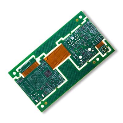
Rigid-flex PCBs: These hybrid PCBs combine rigid and flexible sections in a single circuit board. The rigid sections provide mechanical support and allow for the mounting of larger components, while the flexible sections enable the PCB to bend and fold as needed. Rigid-flex PCBs are commonly used in applications that require both flexibility and stability, such as wearable devices and automotive electronics.

Advantages of Flexible PCBs
Flexible PCBs offer several key advantages over traditional rigid PCBs, making them an attractive choice for many applications:
Space and Weight Savings
One of the primary advantages of flexible PCBs is their ability to save space and weight in electronic devices. Because they can bend and fold to fit into tight spaces, flex circuits can be used to create more compact and lightweight designs than would be possible with rigid PCBs. This is especially important in applications where size and weight are critical factors, such as portable devices and aerospace systems.
Increased Reliability
Flexible PCBs are more resistant to vibration and shock than rigid PCBs, making them less likely to fail or break under stress. This increased reliability is due to the flexible nature of the substrate, which allows the circuit to absorb and dissipate mechanical forces without cracking or breaking. As a result, flexible PCBs are often used in applications that are subject to harsh environments or frequent movement, such as automotive electronics and industrial equipment.
Improved Signal Integrity
Flexible PCBs can also provide improved signal integrity compared to rigid PCBs, especially in high-speed applications. Because the traces on a flex circuit are closer together and have a more consistent dielectric constant, they can reduce signal distortion and crosstalk. This can lead to better overall performance and reliability in applications that require high-speed data transmission, such as telecommunications and networking equipment.
Enhanced Design Freedom
The ability of flexible PCBs to bend and fold allows for greater design freedom and creativity in electronic devices. Designers can use flex circuits to create unique and innovative form factors that would be impossible with rigid PCBs, such as curved displays and wearable devices. This enhanced design freedom can also lead to more ergonomic and user-friendly products, as flex circuits can be shaped to fit the contours of the human body or other objects.
Cost Savings
While flexible PCBs may have a higher initial cost than rigid PCBs due to the specialized materials and manufacturing processes involved, they can actually lead to cost savings in the long run. By enabling more compact and lightweight designs, flex circuits can reduce the overall size and weight of electronic devices, which can lower shipping and transportation costs. Additionally, the increased reliability and durability of flexible PCBs can reduce the need for repairs and replacements, further lowering the total cost of ownership.

Disadvantages of Flexible PCBs
Despite their many advantages, flexible PCBs also have some disadvantages that should be considered when deciding whether to use them in a particular application:
Higher Initial Cost
As mentioned earlier, flexible PCBs typically have a higher initial cost than rigid PCBs due to the specialized materials and manufacturing processes involved. The flexible substrate, such as polyimide or polyester, is more expensive than the standard FR-4 material used in rigid PCBs. Additionally, the manufacturing process for flexible PCBs requires more steps and specialized equipment, such as laser drilling and plasma etching, which can add to the overall cost.
Limited Component Options
Another disadvantage of flexible PCBs is that they have limited options for component mounting compared to rigid PCBs. Because the substrate is flexible, it cannot support heavy or large components without additional reinforcement or stiffeners. This means that certain types of components, such as through-hole components and large connectors, may not be suitable for use on a flex circuit. Instead, surface-mount components and smaller connectors are typically used, which can limit the overall functionality and complexity of the design.
Challenging Assembly Process
The assembly process for flexible PCBs can also be more challenging than for rigid PCBs, especially when it comes to soldering and inspection. Because the substrate is flexible, it can be difficult to keep the components in place during soldering, which can lead to misalignment or poor connections. Additionally, the flexibility of the circuit can make it harder to inspect for defects or errors, as the traces and components may not be visible from all angles.
Reduced Thermal Dissipation
Flexible PCBs also have reduced thermal dissipation compared to rigid PCBs, which can be a problem in applications that generate a lot of heat. Because the substrate is thin and flexible, it does not conduct heat as well as the thicker and more rigid FR-4 material used in standard PCBs. This means that heat-generating components, such as power transistors and processors, may require additional cooling measures or heat sinks to prevent overheating and damage to the circuit.
Limited Current Carrying Capacity
Finally, flexible PCBs have a limited current carrying capacity compared to rigid PCBs, which can be a constraint in high-power applications. The thin traces and substrate of a flex circuit cannot handle as much current as the thicker traces and planes of a rigid PCB, which can lead to voltage drops and power losses. This limitation can be mitigated to some extent by using wider traces or multiple layers, but it still needs to be taken into account when designing a flexible PCB for a high-power application.

Manufacturing Process for Flexible PCBs
The manufacturing process for flexible PCBs is similar to that of rigid PCBs, but with some additional steps and considerations to accommodate the flexible substrate and components:
-
Substrate Preparation: The first step in the manufacturing process is to prepare the flexible substrate, which is typically made from a polymer material such as polyimide or polyester. The substrate is cleaned and treated to improve its adhesion to the conductive traces and components.
-
Circuit Design and Patterning: The next step is to design the circuit and create a pattern for the conductive traces and pads. This is typically done using computer-aided design (CAD) software, which generates a digital file that can be used to control the manufacturing equipment.
-
Copper Lamination: Once the substrate is prepared and the circuit pattern is created, a thin layer of copper is laminated onto one or both sides of the substrate using heat and pressure. The copper layer is typically 18-35 microns thick, depending on the application and design requirements.
-
Photolithography: The copper-laminated substrate is then coated with a photoresist material and exposed to UV light through a photomask that contains the circuit pattern. The exposed areas of the photoresist are hardened and the unexposed areas are washed away, leaving a pattern of exposed copper on the substrate.
-
Etching: The exposed copper is then etched away using a chemical solution, leaving only the desired conductive traces and pads on the substrate. The remaining photoresist is then stripped away, revealing the completed circuit pattern.
-
Coverlay Application: To protect the circuit and improve its durability, a coverlay material is applied over the traces and pads. The coverlay is typically made from a similar polymer material as the substrate and is laminated onto the circuit using heat and pressure.
-
Component Assembly: The final step in the manufacturing process is to assemble the components onto the flexible PCB. This is typically done using surface-mount technology (SMT), where the components are placed onto the pads and soldered in place using a reflow oven or other soldering equipment.
Applications of Flexible PCBs
Flexible PCBs have a wide range of applications across various industries and sectors, from consumer electronics to medical devices and aerospace systems. Here are some examples of common applications for flexible PCBs:
| Industry | Applications |
|---|---|
| Consumer Electronics | – Smartphones and tablets – Wearable devices (smartwatches, fitness trackers) – Cameras and camcorders – Gaming consoles and controllers |
| Medical Devices | – Implantable devices (pacemakers, neurostimulators) – Diagnostic equipment (ultrasound probes, endoscopes) – Wearable health monitors (ECG, EEG) – Surgical instruments and robotics |
| Automotive Electronics | – Dashboard displays and controls – Sensors and actuators (accelerometers, pressure sensors) – Wiring harnesses and connectors – Infotainment and navigation systems |
| Aerospace and Defense | – Avionics and flight control systems – Satellite and spacecraft electronics – Radar and communication equipment – Weapon systems and targeting devices |
| Industrial and Robotics | – Motor controls and drives – Sensors and instrumentation – Robotic arms and grippers – Automation and process control systems |
Designing with Flexible PCBs
Designing with flexible PCBs requires some additional considerations and challenges compared to designing with rigid PCBs. Here are some key factors to keep in mind when designing a flexible PCB:
Bend Radius and Flexibility
One of the most important considerations when designing a flexible PCB is the bend radius and flexibility of the circuit. The bend radius is the minimum radius that the PCB can be bent without damaging the traces or components, and it is typically specified by the manufacturer based on the substrate material and thickness. Designers need to ensure that the bend radius is sufficient for the intended application and that the circuit can flex and move as needed without breaking or losing connectivity.
Trace Width and Spacing
Another key consideration when designing a flexible PCB is the width and spacing of the conductive traces. Because the substrate is thin and flexible, the traces need to be wide enough to carry the required current and prevent voltage drops, but not so wide that they become too stiff or brittle. The spacing between traces also needs to be carefully controlled to prevent crosstalk and signal interference, especially in high-speed applications.
Component Selection and Placement
Selecting and placing components on a flexible PCB can also be challenging, as the components need to be able to withstand the bending and flexing of the circuit without becoming damaged or dislodged. Surface-mount components are typically used, as they have a lower profile and can be more securely attached to the substrate. The placement of the components also needs to be optimized to minimize stress and strain on the circuit, especially in areas where the PCB will be bent or folded.
Stiffeners and Reinforcements
In some cases, it may be necessary to add stiffeners or reinforcements to the flexible PCB to provide additional support and stability for larger or heavier components. Stiffeners are typically made from a rigid material, such as FR-4 or metal, and are attached to the back side of the PCB in areas where the components are mounted. Reinforcements, such as adhesive backing or laminated layers, can also be used to increase the overall strength and durability of the circuit.
Connectors and Interfaces
Finally, designers need to consider how the flexible PCB will interface with other components and systems, both mechanically and electrically. Connectors and interfaces need to be selected and designed to accommodate the flexibility and movement of the circuit, while still providing a secure and reliable connection. This may require the use of specialized connectors or strain reliefs that can flex and bend with the PCB without becoming damaged or disconnected.
Challenges and Considerations
While flexible PCBs offer many advantages and benefits, they also come with some challenges and considerations that need to be taken into account when deciding whether to use them in a particular application:
Cost and Availability
As mentioned earlier, flexible PCBs typically have a higher initial cost than rigid PCBs due to the specialized materials and manufacturing processes involved. This cost can be a barrier for some applications, especially those with tight budgets or low volumes. Additionally, the availability of flexible PCBs may be limited compared to rigid PCBs, as not all manufacturers have the capability or expertise to produce them.
Design Complexity and Expertise
Designing with flexible PCBs can also be more complex and challenging than designing with rigid PCBs, as there are additional factors and considerations to take into account, such as bend radius, trace width and spacing, and component selection and placement. This complexity may require additional expertise and experience on the part of the designer, as well as more advanced design tools and software.
Manufacturing and Assembly
The manufacturing and assembly process for flexible PCBs can also be more challenging and time-consuming than for rigid PCBs, due to the additional steps and equipment involved. This can lead to longer lead times and higher costs, especially for small or prototype quantities. Additionally, the assembly process may require specialized equipment or techniques, such as vacuum or pressure-assisted soldering, to ensure good connections and prevent damage to the components or substrate.
Testing and Inspection
Testing and inspecting flexible PCBs can also be more difficult than rigid PCBs, due to the flexibility and movement of the circuit. Traditional testing methods, such as bed-of-nails or flying probe testing, may not be suitable for flexible PCBs, as the probes can damage or deform the substrate. Instead, specialized testing equipment or techniques, such as 3D X-ray inspection or boundary scan testing, may be needed to ensure the quality and reliability of the circuit.
Durability and Reliability
Finally, the durability and reliability of flexible PCBs can be a concern in some applications, especially those with harsh environments or frequent movement. While flexible PCBs are generally more resistant to vibration and shock than rigid PCBs, they can still be susceptible to damage or failure if not designed or manufactured properly. Designers need to carefully consider the expected operating conditions and lifetime of the circuit, and select materials and components that can withstand the stresses and strains of the application.
Frequently Asked Questions (FAQ)
- What is the difference between a flexible PCB and a rigid PCB?
-
A flexible PCB is made from a thin, flexible substrate material that allows the circuit to bend and flex, while a rigid PCB is made from a thicker, more rigid material that does not allow for any flexibility. Flexible PCBs are typically used in applications where space is limited or where the circuit needs to conform to a particular shape or form factor, while rigid PCBs are used in more traditional, box-shaped electronic devices.
-
What are the most common materials used for flexible PCBs?
-
The most common materials used for flexible PCBs are polyimide (PI) and polyester (PET). Polyimide is a high-performance polymer that offers excellent thermal and mechanical properties, as well as good chemical resistance and dimensional stability. Polyester is a lower-cost alternative that is suitable for less demanding applications, but may not have the same level of performance or durability as polyimide.
-
Can flexible PCBs be used in high-temperature applications?
-
Yes, flexible PCBs can be used in high-temperature applications, but the choice of substrate material and components is critical. Polyimide is typically the preferred material for high-temperature applications, as it can withstand temperatures up to 400°C. However, the components and solder used on the PCB must also be rated for high temperatures, and the design must take into account any thermal expansion or contraction that may occur.
-
How do I choose the right bend radius for my flexible PCB?
-
The bend radius of a flexible PCB is typically specified by the manufacturer based on the substrate material and thickness, as well as the copper weight and any stiffeners or reinforcements used. As a general rule, the minimum bend radius should be at least 6-10 times the thickness of the PCB, but this can vary depending on the specific application and design. It is important to work closely with the PCB manufacturer to determine the appropriate bend radius for your particular application.
-
Can flexible PCBs be repaired or reworked?
- Repairing or reworking a flexible PCB can be more challenging than a rigi


Leave a Reply