Introduction to PCB Manufacturing
Printed Circuit Board (PCB) manufacturing is a complex process that involves several stages, from design to final assembly. To ensure the production of high-quality PCBs, it is essential to consider various factors throughout the manufacturing process. This article will discuss the recommended points to note in PCB manufacturing, covering aspects such as design considerations, material selection, fabrication techniques, quality control, and testing.
PCB Design Considerations
Schematic Design
The first step in PCB manufacturing is creating a schematic design. This design should include all the necessary components, their connections, and the overall circuit layout. When designing the schematic, consider the following points:
- Use standard component symbols and designators
- Ensure proper connections between components
- Minimize the number of crossovers and jumpers
- Consider power supply requirements and decoupling capacitors
PCB Layout Design
Once the schematic design is complete, the next step is to create the PCB layout. The layout determines the physical placement of components and the routing of traces on the board. Keep the following points in mind when designing the PCB layout:
- Choose the appropriate board size and shape
- Determine the number of layers required
- Place components strategically to minimize signal interference
- Use appropriate trace widths and spacing based on signal requirements
- Consider thermal management and power distribution
- Incorporate design for manufacturability (DFM) guidelines

Material Selection
PCB Substrate Materials
The choice of PCB substrate material depends on the application, operating environment, and performance requirements. Common substrate materials include:
| Material | Description | Applications |
|---|---|---|
| FR-4 | Glass-reinforced epoxy laminate | General-purpose, low-cost |
| High Tg FR-4 | FR-4 with higher glass transition temperature | High-reliability, automotive, aerospace |
| Polyimide | High-temperature, flexible material | Flexible circuits, aerospace, military |
| Aluminum | Metal-core PCB for thermal management | High-power LEDs, power electronics |
Consider the following factors when selecting the substrate material:
- Dielectric constant and loss tangent
- Thermal conductivity and coefficient of thermal expansion (CTE)
- Mechanical strength and flexibility
- Cost and availability
Copper Foil Thickness
The thickness of the copper foil used in PCB manufacturing affects the current carrying capacity and signal integrity of the traces. Standard copper foil thicknesses include:
| Thickness (oz) | Thickness (µm) | Current Carrying Capacity (A/mm) |
|---|---|---|
| 0.5 oz | 17.5 µm | 0.5 A/mm |
| 1 oz | 35 µm | 1.0 A/mm |
| 2 oz | 70 µm | 2.0 A/mm |
Choose the appropriate copper foil thickness based on the current requirements and signal integrity needs of your design.

PCB Fabrication Techniques
Etching Methods
PCB fabrication involves etching away unwanted copper to form the desired traces and pads. The two primary etching methods are:
-
Subtractive Etching: This method involves removing copper from a fully copper-clad board using a photoresist and etchant. It is suitable for simple designs with larger feature sizes.
-
Additive Etching: In this method, copper is selectively added to the board using electroplating or electroless plating. Additive etching allows for finer feature sizes and is suitable for complex designs.
Drilling and Plating
After etching, holes are drilled in the PCB for component leads and vias. The drilled holes are then plated with copper to establish electrical connections between layers. Consider the following points during drilling and plating:
- Use appropriate drill bit sizes and speeds
- Ensure proper registration between layers
- Control the plating thickness and uniformity
- Inspect for drill breakouts and plating voids
Solder Mask and Silkscreen
Solder mask is a protective coating applied to the PCB surface to prevent solder bridging and provide insulation. Silkscreen is used to print component designators, logos, and other markings on the board. When applying solder mask and silkscreen, keep the following points in mind:
- Choose the appropriate solder mask color (green, black, white, etc.)
- Ensure proper alignment and registration of silkscreen
- Verify the accuracy of component designators and markings
- Consider the minimum solder mask thickness and clearance requirements

Quality Control and Testing
Visual Inspection
Visual inspection is the first step in quality control and involves examining the PCB for obvious defects such as:
- Broken or missing traces
- Short circuits or open circuits
- Incorrect component placement
- Solder mask or silkscreen errors
Use magnification and adequate lighting to perform thorough visual inspections.
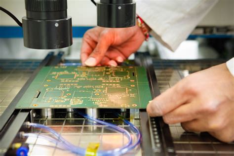
Automated Optical Inspection (AOI)
AOI uses computer vision and image analysis to detect manufacturing defects on the PCB. AOI systems can identify issues such as:
- Solder bridges or shorts
- Component misalignment or absence
- Insufficient or excessive solder
- Trace width or spacing violations
Implement AOI at various stages of the manufacturing process to catch defects early and reduce rework costs.
Electrical Testing
Electrical testing verifies the functionality and performance of the PCB. Common electrical tests include:
- Continuity Test: Checks for open circuits and short circuits between nets.
- Insulation Resistance Test: Measures the resistance between isolated conductors to ensure adequate insulation.
- High-Potential (HiPot) Test: Applies a high voltage between conductors to detect insulation breakdowns or leakage currents.
- Functional Test: Verifies the PCB’s operation under normal and extreme conditions using test fixtures or flying probe testers.
Perform electrical testing at various stages, such as bare board testing, in-circuit testing, and final functional testing.
FAQs
1. What is the minimum feature size achievable in PCB manufacturing?
The minimum feature size depends on the PCB fabrication technology and the manufacturer’s capabilities. Typical minimum feature sizes are:
- Standard PCB: 6 mil (0.15 mm) trace width and spacing
- Advanced PCB: 3 mil (0.075 mm) trace width and spacing
- HDI PCB: 2 mil (0.05 mm) trace width and spacing
2. How can I minimize signal integrity issues in my PCB design?
To minimize signal integrity issues, follow these guidelines:
- Use appropriate trace widths and spacing based on signal frequency and impedance requirements
- Minimize the length of high-speed signal traces
- Use ground planes and proper grounding techniques
- Implement appropriate termination and impedance matching
- Consider the use of differential signaling for high-speed interfaces
3. What are the advantages of using a 4-layer PCB over a 2-layer PCB?
A 4-layer PCB offers several advantages over a 2-layer PCB:
- Improved signal integrity due to dedicated power and ground planes
- Better EMI/EMC performance
- Increased routing density and design flexibility
- Enhanced thermal management and heat dissipation
4. How can I ensure the manufacturability of my PCB design?
To ensure the manufacturability of your PCB design, follow these steps:
- Adhere to the manufacturer’s design guidelines and constraints
- Use standard component package sizes and footprints
- Provide adequate clearances and tolerances for traces, pads, and holes
- Minimize the use of vias and blind/buried vias
- Perform design rule checks (DRC) and correct any violations
5. What are the environmental factors to consider when selecting PCB materials?
When selecting PCB materials, consider the following environmental factors:
- Operating temperature range
- Humidity and moisture resistance
- Chemical and solvent resistance
- Mechanical stress and vibration
- Flammability and thermal shock resistance
Choose materials that can withstand the expected environmental conditions to ensure the long-term reliability of your PCB.
Conclusion
PCB manufacturing is a complex process that requires careful consideration of various factors, from design to assembly. By following the recommended points discussed in this article, you can ensure the production of high-quality, reliable PCBs that meet your application requirements. Remember to prioritize design for manufacturability, select appropriate materials, and implement robust quality control and testing procedures throughout the manufacturing process.


Leave a Reply