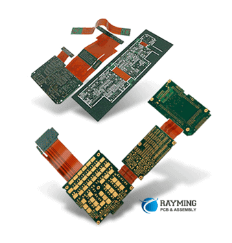
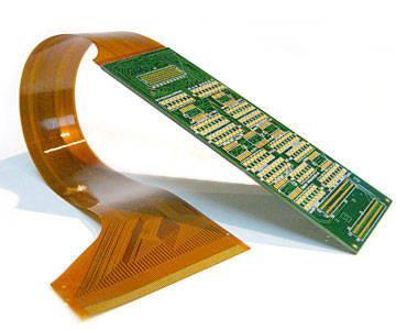
What is Rigid Flex PCB?
A rigid flex PCB (also known as rigid flex circuit board or flex-rigid PCB) is a printed circuit board that consists of multiple layers of flexible polymer and rigid FR4 laminates. These circuit boards provide flexibility in certain areas of the PCB while maintaining rigidity in others, allowing the board to bend and flex to fit unique form factors and enclosures.
Rigid flex PCBs integrate the best qualities of both rigid PCBs and flex circuits into a single design. They provide:
- Mechanical flexibility to fit and move within constrained spaces
- Durability and rigidity for areas that require structural support
- Reliable connections between multiple PCB assemblies
- Miniaturization and space savings
- Reduced system wiring and connectors
With their ability to fold, wrap, and flex, rigid flex PCBs are ideal for products like mobile devices, wearables, medical devices, industrial electronics, and automotive electronics.
Benefits of Using Rigid Flex PCBs
Here are some of the key benefits that rigid flex PCB technology provides:
Size and Space Savings
By integrating flexible folds and connections, rigid flex PCBs can compact and condense PCB assemblies that would normally require external cables and connectors. This allows for smaller product sizes.
Flexibility and Movement
The flex sections of the PCB allow it to bend, twist, and flex to move dynamically within an assembly. This is critical in space-constrained devices.
Reliability
Rigid flex PCBs have very reliable connections between rigid sections, eliminating connectors and solder joints that can fail.
Adaptability
Rigid flex PCBs can be designed with custom shapes, bends, and folds to fit specialized mechanical assemblies.
Reduced System Complexity
Consolidating PCBs into a single rigid flex assembly simplifies the electronics and reduces overall parts count.
Enhanced Signal Integrity
Shorter trace lengths, fewer connectors, and continuous shielding in rigid flex PCBs enhances signal performance.
Design Freedom
Rigid flex allows more freedom and flexibility (pun intended) in electronics layout and industrial design. Components can be placed optimally.
Common Applications of Rigid Flex PCBs
Here are some of the products and applications that typically utilize rigid flex PCB technology:
- Wearable electronics – smart watches, fitness bands, health trackers, VR headsets
- Mobile phones – cell phones, smartphones
- Tablets and laptops – touchscreen devices
- Medical devices – imaging equipment, monitors, probes
- Automotive electronics – sensors, cameras, control units
- Industrial controls – robotics, automation systems, controllers
- Aerospace and defense – avionics, guidance systems, UAVs
Basically any application where small, lightweight, and dynamic circuit boards are required will benefit from utilizing rigid flex PCB technology. The combination of flexibility and rigidity provides many advantages.
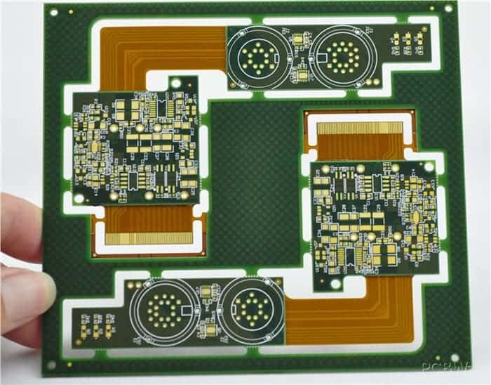
Rigid Flex PCB Construction
Rigid flex PCBs have a complex multilayer construction that requires specialized materials and fabrication techniques. Here is an overview of the construction:
- Flexible substrate – the flex sections use a polyimide film flexible dielectric layer, such as Kapton or Upilex. These films can be 25 to 100 microns thick.
- Rigid substrate – the rigid sections use standard glass reinforced FR-4 material or similar rigid laminates. Common thicknesses are 0.4mm to 2.0mm.
- Adhesive layers – Bonding films like acrylic or epoxy are used to laminate the flexible and rigid layers together into a complete circuit board.
- Copper layers – Polyimide flex layers use extremely thin copper (9 to 18 microns). Rigid FR4 sections use standard 1oz to 2oz copper (35 to 70 microns).
- Cover layers – Additional polyimide, FR4, or other laminates are bonded to the top and bottom to enclose internal layers.
- Stiffeners – Special islands of rigid fiberglass are added for structural stability.
- ** Silkscreen** – Printed solder masks, nomenclature, and other markings for identification and aesthetics.
Rigid sections typically make up 70% or more of the board area, with flex sections in narrower areas and folds between rigid regions.
Rigid Flex PCB Design Rules
Designing and laying out rigid flex PCBs requires special considerations and rules to ensure manufacturability, reliability, and performance. Here are some key rigid flex design guidelines:
- Layer stackup – Must have a symmetric sequence of layers on both sides of center-plane for stability. Similar rigid and flex layer thicknesses must align.
- Rigid-to-flex transitions – Use teardrop shapes and tapers at least 200 mils long to transition rigid to flex without gaps or material fractures.
- Bend radius – Avoid tight folds; maintain at least a 2:1 ratio of bend diameter to board thickness.
- Flex reinforcement – Add stiffeners or additional layers in high-stress flex areas.
- Components placement – Avoid placing heavy components in unstable flex areas. Distribute weight evenly.
- Trace routing – Route signals primarily on inner layers; use outer layers for power/ground. Avoid fracturing traces at bends.
- Vias – Use flex-specific filled vias. Do not place unfilled vias in dynamic or high-stress areas.
- Spacing and clearance – Increase spacing between traces, pads, and features due to alignment variability.
Rigid flex PCB layouts require specialized CAD tools with rigid-flex board capabilities, such as Mentor Xpedition, Cadence Allegro, and Altium Designer.
Rigid Flex PCB Manufacturing Process
Producing rigid flex PCBs requires a combination of standard PCB fabrication techniques along with some additional steps:
1. Circuit Design and Layout
Just like any PCB, the first step is schematic capture and board layout using EDA tools. The CAD tools must support rigid-flex board design.
2. Material Preparation
The rigid and flexible core layers are prepared. Rigid cores are processed similar to a standard PCB. Flex cores require additional steps like sputtering thin copper and cleaning.
3. Imaging
Rigid sections are imaged using standard lithography processes. Flexible sections require laser direct imaging to define traces on the thin flexible copper layers.
**4. Layer Bonding **
Sections are bonded together through layup, lamination, and adhesive pressing using high temperatures and pressures. Special fixtures hold layers in alignment.
5. Via Formation
Mechanically drilled and stacked vias are used in rigid sections. Laser or plasma ablation creates vias in the thin flexible layers.
**6. Outer Layer Imaging **
Lithography and printing forms the outer layer traces, pads, solder mask, nomenclature, etc. Flex and rigid sections are selectively processed.
7. Testing and Finishing
Electrical testing validates connectivity. Hardware insertion, solder mask curing, edge trimming, and other finishing steps complete fabrication.
8. Assembly
Components are soldered onto the board using SMT and through-hole assembly processes. Care is taken in handling flex areas.
Rigid flex PCB manufacturing requires advanced skills, special equipment, tight process controls, and often extensive prototyping to hone designs and processes. Costs are typically much higher compared to standard PCBs.
Rigid Flex PCB Assembly and Integration
In addition to the standard PCB assembly process, assembling components onto rigid flex boards requires some special handling and integration steps:
- Parts should be glued or anchored in flex areas to prevent movement and fracturing
- Kapton tape or other reinforcement should be added to high-stress flex bends
- Avoid placing connectors, switches, or heavy parts in unstable sections
- Use flexible solder, conductive epoxy, or isopropyl alcohol for flex area attachments
- Manual and dedicated feeders should be used for odd-shaped boards
- Special fixtures may be needed for supporting boards during assembly
- Protect flex areas against bending and kinking during handling
- Allow sufficient clearance for free movement of rigid sections
With care taken during assembly, rigid flex PCBs enable unique designs, miniaturization, and enhanced reliability for products where flexibility, space savings, and adaptability are critical requirements.
Rigid Flex PCB Failure Modes
While extremely capable, rigid flex PCBs may encounter certain failure modes if not designed and manufactured correctly:
- Flex fracture – Traces crack over repeated bending stress. Mitigate with proper bend radius and support.
- Delamination – Layers separate due to excessive flexing or impact. Ensure proper adhesion and handling.
- Tear out – Inadequate reinforcements and spacing around drilled vias can lead to pad lift off and connections ripping.
- Fatigue – Repeated bending in the same area causes material weakening and eventual interconnect failure.
- Shorts – Exposure during flexing can allow short circuits between traces and pads. Maintain adequate spacing and insulation.
- Cracks – Flexing can propagate cracks in surface mount pads and components leads. Use flexible parts and anchors.
With good design, material selection, prototyping, and process validation, potential failure modes can be identified and mitigated to ensure a robust, reliable rigid flex PCB assembly.
Rigid Flex PCB Variations
There are many possible variations to the basic rigid flex design to meet specialized requirements:
- Multilayer rigid flex – 12+ layer counts are possible with complex inner layer rigid and flex substrates
- Rigid-flex-rigid – Combines multiple rigid boards joined by flex sections
- Sculpted rigid flex – Complex 3D shapes molded into the rigid sections
- Metal core rigid-flex – Metal substrate inner layers for thermal management
- Flexible stiffeners – Special flexible stiffener materials replace rigid islands
- Flexible-on-rigid – Thin flex layers selectively attached to rigid substrate
- Sequential lamination – Separate rigid and flex fabrication, then combined
- Molded interconnect devices – Components molded into flexible material
The implementation options for rigid flex PCBs are vast to accommodate highly challenging and custom electronic designs.
Rigid Flex PCB FAQs
Here are answers to some frequently asked questions about rigid flex PCBs:
Q: What are some key considerations in rigid flex PCB design?
A: Trace routing, layer stack planning, component placement, managing transitions between rigid and flex, controlling bend radii, and handling vias/holes are critical considerations.
Q: What types of materials are used in rigid flex PCB construction?
A: Polyimide films are used for the flexible layers. FR4 glass reinforced laminates are used for the rigid sections. Adhesives bond the layers.
Q: How many bend cycles can a rigid flex PCB support?
A: Depending on materials and construction, rigid flex boards can typically withstand 500 to 10,000+ flex cycles before failure.
Q: What are the limitations of rigid flex PCB technology?
A: Limitations include higher cost, design complexity, specialized fabrication, potential reliability issues, and constrained capabilities for high-frequency or high-speed signals.
Q: What are some examples of rigid flex PCB applications?
A: Mobile phones, tablets, wearables, medical devices, industrial controls, aerospace avionics, and automotive electronics all utilize rigid flex PCBs extensively.
I hope this overview has provided a comprehensive introduction to rigid flex PCB technology and manufacturing processes. Please let me know if you need any clarification or have additional questions!


Leave a Reply