Introduction to Polyimide Flex PCBs
A polyimide flex PCB (flexible printed circuit board) is a type of PCB made with polyimide base material. Polyimide is a type of plastic polymer material known for its heat and chemical resistance as well as its flexibility.
Polyimide flex PCBs allow for dynamic movement and flexing applications compared to traditional rigid PCBs. They are ideal for use in space-constrained and movable products like wearables, medical devices, automotive electronics and more.
Some key advantages of polyimide flex PCBs include:
- Flexibility – Polyimide flex circuits can bend and flex repeatedly without damage. This makes them perfect for dynamic applications.
- Lightweight – Polyimide flex PCBs are extremely lightweight and thin. Their low mass makes them well-suited for mobile devices.
- Durability – The polyimide material offers high resistance to heat, cold and chemicals. Polyimide flex PCBs are very durable.
- High density – Flex PCBs allow for more compact and dense circuit designs by folding and stacking layers.
- Soft – The flexibility allows for a softer, more comfortable feel and interface with human body.
- Reliability – Well-designed flex PCBs are reliable for complex flexible applications.
In this in-depth guide, we’ll cover everything you need to know about polyimide flex PCBs including types, design rules, manufacturing processes, applications and more.
Types of Polyimide Flex PCBs
There are two main types of polyimide flex PCBs classified by the number of conductive layers:
Single Layer Flex PCBs
- One conductive layer
- Typically a thin polyimide layer around 25-50 microns thick
- Often used for simple low complexity flex circuits like membrane switches
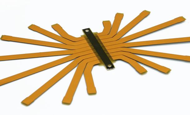
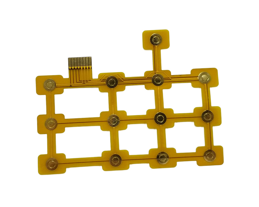
Multilayer Flex PCBs
- Multiple conductive layers (2 to over 10 layers)
- Layer thickness around 50-100 microns thick
- Allows for more complex high density flex PCB designs
- Layers can be stacked and folded to save space
Within these two main categories, there are additional types of polyimide flex PCBs designed for specific applications:
- Rigid-flex PCBs – Combines rigid and flexible substrates into a single circuit board. Allows flexible “hinges” between rigid regions.
- Metal-backed flex – Polyimide flex PCB with attached metal stiffener for rigidity and EMI/EMC shielding.
- Flex-rigid-flex – Special rigid-flex with flexible sections on both sides of a rigid PCB area.
- Sculpted flex – Flex PCB etched into various 2D or 3D shapes conforming to product surfaces.
Polyimide Material Types
The most common polyimide base materials used in flex PCB manufacturing include:
- Kapton – Developed by DuPont, Kapton is one of the most widely used polyimide films. Offers high heat and chemical resistance.
- UPILEX – Ube Industries polyimide film alternative to Kapton with similar performance and properties.
- Upilex-S – Modified version of UPILEX with improved dimensional stability for rigid-flex boards.
- Apical – Polyimide film from Kaneka that can withstand higher temperatures than Kapton or UPILEX.
Design Guidelines for Polyimide Flex PCBs
Designing a polyimide flex PCB requires following certain guidelines and rules to ensure the circuit can bend and move reliably. Key guidelines include:
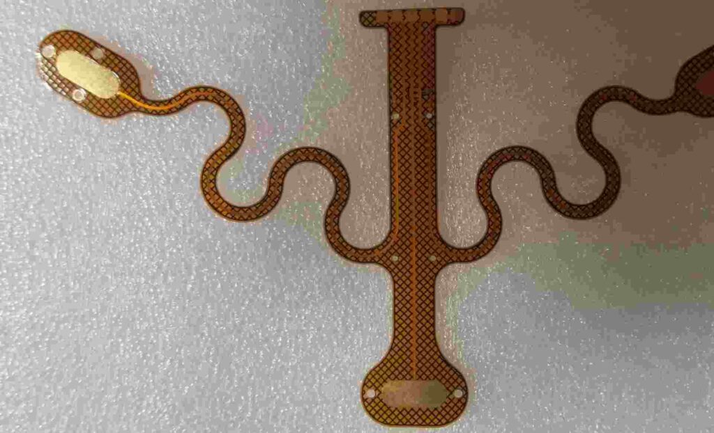
Flexible Regions
- Minimize components in flexible areas to avoid damage from flexing stress.
- Avoid 90 degree bends. Use large bend radii of at least 10X material thickness.
- Strategically place flex joints along the neutral axis to minimize strain.
Trace Routing
- Use large trace widths and clearances for better reliability. Minimum 5 mil trace/space.
- Avoid thin neck-down traces that can break under dynamic bending.
- Route traces in the direction of the bend axis for minimal flex stress.
Stiffeners and Supports
- Add stiffeners on layers near outer surfaces for rigidity and to prevent flex cracks.
- Use covers, shields or metal backing for protection and rigidity.
Adhesives
- Use flex-grade non-conductive adhesives optimized for dynamic bending apps.
- Anchor stiff components near the rigid areas and away from high flex zones.
Vias
- Use staggered pattern for vias instead of single rows in flex areas.
- Fill vias with flex-grade dielectric to avoid cracking under bending loads.
Flex PCB Layout
- Orient components for optimal compact layout and trace routing.
- Place connectors and testpoints in rigid areas with no or minimal flexing.
- Distribute components evenly to prevent imbalance and twisting.
Polyimide Flex PCB Material Stackup
A polyimide flex PCB will have a specific material stackup depending on the number of conductive layers. Here are some typical layer compositions:
Single Layer Flex PCB
- Polyimide Base Layer: Flexible substrate layer. Kapton or UPILEX. 25-100 micron thickness.
- Adhesive: Bonds base layer to copper. Flex-grade acrylic or epoxy adhesive.
- Copper Layer: 18-35 μm electrodeposited copper. Single conductive layer.
- Coverlay: Flexible solder mask layer for protection. 25-50 μm thick.
Two Layer Flex PCB
- Polyimide Base Layers: Kapton or UPILEX films on both sides. 50-100 μm thick each.
- Adhesive: Bonds polyimide base layers to copper. Flex-grade acrylic or epoxy.
- Copper Layers: 18-35 μm copper on each side. 2 total conductive layers.
- Coverlay: Thin solder mask coverlay for protection.
Multilayer Flex PCB
- Multiple alternating layers of polyimide dielectric films and copper foil.
- Bonded together with acrylic or epoxy adhesive.
- Number of layers can be 4, 6, 8, 10 or more.
- Allows for denser, more complex flex PCB design.
- Thickness around 100-200 μm.
The polyimide base material gives the flex PCB its flexible properties. The adhesive permanently bonds the layers together. Etched copper foils form the conductive traces and pads. Coverlay or soldermask coats and protects the external layers.
Polyimide Flex PCB vs Rigid-Flex PCBs
Polyimide flex PCBs provide full flexibility while rigid-flex PCBs offer a combination of both flexible and rigid sections.
Some key differences between pure polyimide flex PCBs and rigid-flex boards:
| Polyimide Flex PCB | Rigid-Flex PCB |
|---|---|
| Fully flexible construction | Combines rigid board material (FR4) with flexible polyimide |
| Thin polyimide base layer | Rigid sections have thicker FR4 dielectric |
| Dynamic repeated bending | Flexible “hinges” between rigid regions |
| Lightweight, low profile | Heavier and thicker due to rigid portions |
| Lower complexity circuits | Can support higher complexity circuits |
| Mainly for simple flex movement | Ideal for complex motion requiring both flex and rigidity |
Rigid-flex PCBs contain expensive laser-drilled microvias to connect layers. This fabrication complexity increases costs compared to pure flex PCBs.
For applications only requiring simple flexing, an all polyimide flex PCB is preferable. Rigid-flex PCBs allow combining intricate rigid PCBs with dynamic flex joints.
Polyimide Flex PCB Manufacturing Process
Specialized processes are required to manufacture polyimide flex PCBs. Here is an overview of the typical flex PCB fabrication workflow:
Design and Layout
- Create flex PCB design following IPC guidelines for trace spacing, annular rings, etc.
- Use CAD tools like Altium or Cadence for optimal flex design layout.
- Simulate design to verify bend radius, trace stresses and reliability.
Material Selection
- Choose flex-grade polyimide type – Kapton, UPILEX, etc.
- Determine base material thickness based on required flexibility.
- Select adhesive type like acrylic or epoxy to bond layers.
Imaging
- Photolithography transfers circuit image onto photoresist coated layers.
- Advanced laser direct imaging (LDI) techniques can also be used.
- Highly accurate imaging to define fine features on flex PCB.
Etching
- Etch away unwanted copper to leave behind desired traces and pads.
- Etching done with chemical solutions or plasma etching.
- Clean residues and coat with soldermask coverlay.
Layer Bonding
- Align layers and laminate together using heat and pressure.
- Adhesive permanently bonds the layers into full flex stackup.
- Multilayer builds may require sequential bonding of sub-assemblies.
Testing and Inspection
- Test for shorts, opens and verify impedance.
- Inspect board dimensions, bends, registration accuracy.
- Ensure flex PCB meets all electrical and mechanical requirements.
Singulation
- Depanel boards by cutting individual PCBs from panel frame.
- Common methods like V-scoring or routing.
- Carefully remove to avoid damage during depaneling.
The specialized materials and processes result in a cost premium over rigid PCB fabrication. But the benefits of flexible PCB technology often justify the additional costs for complex flex applications.
Polyimide Flex PCB Applications
Thanks to their flexible properties, polyimide flex PCBs are an enabling technology across many cutting edge applications including:
Wearable Electronics
- Smart watches, fitness bands, health trackers
- Flex circuits conform to wrist and body
- Withstand repeated bending movements
Medical Devices
- Implants, IV catheters, surgical tools
- Thin, lightweight. Won’t irritate internal tissues
- Flexibility suits dynamic body movements
Automotive Electronics
- Instrument clusters, sensors, engine control modules
- Vibration resistance
- Withstand extreme temperatures
- Tight space requirements
Aerospace and Defense
- UAVs, avionics, radars, missiles
- Rugged and durable in harsh environments
- Vibration damping. Noise reduction.
Robotics
- Arms, joints, end effectors
- Foldable flex circuits suit articulated robots
- Repeated dynamic motion and bending
Consumer Electronics
- Phones, laptops, cameras
- Compact form factors
- Flexible interconnects between components
- Feature-rich handheld mobile devices
Polyimide flex PCB technology will continue expanding into innovative applications across many industries that require flexible, dynamic circuitry.
Pros and Cons of Polyimide Flex Circuits
Here is a summary of the key benefits as well as downsides to consider with polyimide flex PCBs:
Polyimide Flex PCB Pros
- Extremely flexible and elastic
- Withstand repeated bending without damage
- Lightweight and low profile design
- Allows dynamic movement and folding
- Excellent thermal stability
- Chemically resistant
- Vibration dampening
- Soft and conformal shape
- High trace densities with multilayer design
- Well suited for complex motion
- Enables compact product designs
Polyimide Flex PCB Cons
- Relatively more expensive than rigid PCBs
- Design constraints around flex zones
- Limited component densities in flex areas
- Fabrication is more complex compared to rigid boards
- Prone to cracking without proper reinforcement
- Requires advanced soldering processes
- Higher level of expertise needed for flex PCB design
- More challenging assembly and inspection after population
- Longer prototyping lead times
Flex PCB Design Tips
Here are some helpful tips when designing a polyimide flex PCB:
- Minimize components in high-flex areas. Place them in static rigid zones.
- Use minimum trace/space rules of 5 mil line/5 mil space.
- Include generous radii on all bends of at least 10X material thickness.
- Strategically place slits or cutouts to promote easier bending in desired direction.
- Clearly indicate rigid sections and flexible sections on the design.
- Simulate dynamic bending and stresses using FEA tools.
- Account for effects of components, coverlay, adhesives on flex stiffness.
- Review the design with your flex PCB manufacturer during the development process.
- Build in several 0.1″ wide testpoints for easy electrical testing.
- Budget extra time for design revisions and multiple prototype iterations.
Polyimide Flex PCB Cost Drivers
What factors affect the costs when quoting and manufacturing polyimide flex PCBs? Here are the primary considerations:
Number of conductive layers – More layers means higher costs to fabricate the multilayer flex PCB stackup.
Tight tolerances – Holding tight registration and feature tolerances drives cost up.
Advanced materials – Using costly polyimide films, adhesives and base metals adds cost.
Special processing – Extra fabrication steps like LDI imaging, complex etching, sequential lamination all add cost.
Low volume – Smaller prototype and NRE volumes mean higher prices per flex PCB.
Reliability testing – Extensive testing and inspection at each process step increases cost.
High complexity – Intricate nested routing, high component densities, fine features add cost.
Special handling – Careful depaneling, population, post-etching processes require extra steps and cost.
Quick-turns – Prioritizing fast delivery of prototypes and small batches adds expense.
Working closely with your flex PCB vendor during design and quoting is important to balance cost drivers with product requirements.
Polyimide Flex PCB FAQs
Here are some commonly asked questions about polyimide flex PCB technology:
Q: What are some typical applications for polyimide flex PCBs?
A: Common applications include wearables, medical devices, robotics, automotive, aerospace, and consumer electronics where dynamic flexing is needed.
Q: What are some key benefits of polyimide flex circuits?
A: Key benefits are flexibility, lightweight design, vibration resistance, high reliability, dense layouts, and ability to integrate complex motion into products.
Q: Are flex PCBs more expensive to manufacture than rigid PCBs?
A: Yes, generally polyimide flex PCB fabrication has a cost premium over rigid circuit boards due to the specialized materials, processes and expertise required.
Q: What are some ways to lower the cost of polyimide flex PCBs?
A: Strategies like reducing layer count, minimizing features/tolerances, increasing panel utilization, and placing larger orders can help lower flex PCB costs.
Q: Can components be mounted onto polyimide flex PCBs?
A: Yes, components can be soldered onto flex PCBs using specialized flex assembly processes. But placement is limited in high-flex zones.
Q: What are some examples of rigid-flex PCB applications?
A: Rigid-flex PCBs are ideal in products like laptops, mobile phones, and medical devices which need both rigid support and dynamic flexing.
Q: How long does it typically take to get polyimide flex PCB prototypes?
A: Depending on design complexity, feature size, and volume, prototyping lead times range from 5-10 days on the quick end up to 4-6 weeks for complex designs.
Conclusion
Polyimide flex PCB technology enables innovative products in a wide range of dynamic flexing applications from wearables to medical devices to robotics.
With their flexible properties, lightweight and reliable design, polyimide flex circuits can transform product functionality and user experience. However, specialized design considerations are required.
Collaborating closely with an experienced flex PCB manufacturer during the design, prototyping and development process is key to ensuring a successful project. With proper design foresight, polyimide flex PCBs provide an optimal interconnect solution for the most demanding flexing applications.


Leave a Reply