Why is PCB Testing Important?
PCB testing is essential for several reasons:
-
Quality Assurance: Testing helps identify defects, short circuits, open circuits, and other issues that may impact the performance of the PCB.
-
Reliability: Thorough testing ensures that the PCB will function as intended under various operating conditions, reducing the risk of failures in the field.
-
Cost Savings: Identifying and fixing issues early in the manufacturing process can save significant costs associated with rework, recalls, and customer dissatisfaction.
-
Compliance: Testing helps ensure that the PCB meets industry standards and regulatory requirements.
Types of PCB Testing
There are several types of PCB tests that can be performed at various stages of the manufacturing process:
1. Visual Inspection
Visual inspection is the first step in PCB testing and involves examining the board for any visible defects, such as:
- Incorrect component placement
- Solder bridges or insufficient solder
- Damaged or missing components
- Contamination or foreign objects
Visual inspection can be performed manually or using automated optical inspection (AOI) systems.
2. Automated Optical Inspection (AOI)
AOI uses high-resolution cameras and image processing software to automatically inspect PCBs for defects. This method is faster and more consistent than manual inspection, and can detect issues such as:
- Component placement errors
- Solder defects (bridges, insufficient solder, etc.)
- Missing or incorrectly oriented components
- Trace width and spacing violations
3. X-Ray Inspection
X-ray inspection is used to examine solder joints and other hidden features that cannot be seen with visual or AOI methods. This technique is particularly useful for inspecting:
- Ball Grid Array (BGA) packages
- Flip-chip devices
- Through-hole components
- Multilayer PCBs
4. In-Circuit Testing (ICT)
ICT is a type of electrical test that verifies the functionality of individual components on the PCB. This test is performed using a bed-of-nails fixture that makes contact with specific points on the board. ICT can detect:
- Component value errors (resistors, capacitors, etc.)
- Incorrect component placement
- Open or short circuits
- Missing or damaged components
5. Flying Probe Testing
Flying probe testing is an alternative to ICT that uses movable probes to make contact with test points on the PCB. This method is more flexible than ICT and does not require a custom fixture, making it suitable for low-volume production and prototypes. Flying probe testing can detect:
- Open and short circuits
- Component value errors
- Incorrect component placement
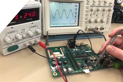
6. Functional Testing
Functional testing verifies that the PCB performs as intended under real-world operating conditions. This type of testing typically involves:
- Applying power to the board
- Providing input signals
- Measuring output signals
- Verifying functionality against design specifications
Functional testing may also include environmental testing, such as temperature cycling, vibration, and humidity exposure.

PCB Testing Techniques
Several techniques can be employed to perform the various types of PCB tests:
1. Boundary Scan Testing
Boundary scan testing, also known as JTAG (Joint Test Action Group) testing, is a method that uses a special test access port (TAP) to control and observe the state of individual pins on a PCB. This technique is useful for testing complex digital circuits and can detect:
- Open and short circuits
- Stuck-at faults
- Interconnect failures
2. Burn-In Testing
Burn-in testing involves subjecting the PCB to elevated temperatures and voltages for an extended period to identify early failures and improve reliability. This technique accelerates the aging process and can reveal:
- Component defects
- Solder joint issues
- Intermittent failures
3. Electromagnetic Compatibility (EMC) Testing
EMC testing verifies that the PCB does not emit excessive electromagnetic interference (EMI) and is not susceptible to external EMI. This type of testing is critical for ensuring compliance with regulatory standards and preventing interference with other electronic devices.
4. Automatic Test Equipment (ATE)
ATE is a computer-controlled system that automates the testing process, allowing for faster, more consistent, and more comprehensive testing. ATE systems can perform various types of tests, including:
- In-circuit testing
- Functional testing
- Boundary scan testing
- Flying probe testing

Best Practices for PCB Testing
To ensure effective and efficient PCB testing, consider the following best practices:
-
Start Testing Early: Incorporate testing into the design process to identify and address issues as early as possible.
-
Develop a Comprehensive Test Plan: Create a detailed test plan that covers all relevant types of tests and defines acceptance criteria.
-
Use Appropriate Test Coverage: Ensure that your test coverage is sufficient to detect all potential defects and verify functionality.
-
Implement Design for Testability (DFT): Design your PCB with testability in mind, incorporating features such as test points, boundary scan chains, and built-in self-test (BIST) capabilities.
-
Maintain Proper Documentation: Keep accurate and up-to-date records of test results, procedures, and any modifications made to the PCB.
-
Continuously Improve: Regularly review and update your testing processes based on lessons learned and new technologies or techniques.

PCB Testing for Prototypes and Low-Volume Production
When testing prototypes or low-volume PCB assemblies, it’s essential to balance the need for thorough testing with the constraints of time and resources. Some strategies for testing prototypes and low-volume production include:
-
Focus on Critical Functionality: Prioritize testing of the most critical functions and components to ensure basic operation and catch major defects.
-
Use Flying Probe Testing: Flying probe testing is more flexible and cost-effective for low-volume production compared to ICT, which requires a custom fixture.
-
Perform Thorough Visual Inspection: Manual visual inspection can be more practical for low-volume production than automated methods like AOI.
-
Leverage Boundary Scan Testing: Boundary scan testing can be an efficient way to test complex digital circuits on prototype PCBs.
-
Consider Outsourcing: Outsourcing PCB testing to a specialized provider can be cost-effective for low-volume production and provide access to advanced testing equipment and expertise.
Frequently Asked Questions (FAQ)
-
What is the difference between ICT and flying probe testing?
In-circuit testing (ICT) uses a bed-of-nails fixture to make contact with specific test points on the PCB, while flying probe testing uses movable probes. ICT requires a custom fixture and is better suited for high-volume production, while flying probe testing is more flexible and cost-effective for low-volume production and prototypes. -
What is boundary scan testing, and when is it used?
Boundary scan testing, also known as JTAG testing, uses a special test access port (TAP) to control and observe the state of individual pins on a PCB. This technique is useful for testing complex digital circuits and is often used when access to test points is limited or when testing high-density PCBs. -
How can I improve the testability of my PCB design?
To improve the testability of your PCB design, consider implementing Design for Testability (DFT) principles, such as adding test points, using boundary scan chains, and incorporating built-in self-test (BIST) capabilities. Additionally, ensure that your design follows best practices for manufacturability and assembly. -
What types of tests are typically performed on prototype PCBs?
When testing prototype PCBs, the focus is usually on verifying critical functionality and catching major defects. Common tests for prototypes include visual inspection, flying probe testing, boundary scan testing, and functional testing. The specific tests performed will depend on the complexity of the PCB and the available resources. -
How do I select the right PCB testing methods for my project?
Selecting the appropriate PCB testing methods depends on several factors, including the complexity of the PCB, the production volume, available resources, and regulatory requirements. Consider the types of defects you need to detect, the level of test coverage required, and the trade-offs between cost, speed, and flexibility when choosing testing methods.
| Test Type | Description | Advantages | Disadvantages |
|---|---|---|---|
| Visual Inspection | Manual or automated examination of PCB for visible defects | Quick and simple; can catch obvious defects | Limited to visible defects; subjective if performed manually |
| Automated Optical Inspection (AOI) | Automated inspection using high-resolution cameras and image processing | Fast and consistent; can detect a wide range of defects | Cannot detect hidden defects; requires programming and setup |
| X-Ray Inspection | Examination of solder joints and hidden features using X-rays | Can detect defects in hidden areas; useful for complex packages and multilayer PCBs | Expensive equipment; requires skilled operators |
| In-Circuit Testing (ICT) | Electrical testing of individual components using a bed-of-nails fixture | Can detect component value errors and placement issues; fast and automated | Requires custom fixture; limited access to test points |
| Flying Probe Testing | Electrical testing using movable probes | Flexible and cost-effective for low-volume production; no custom fixture required | Slower than ICT; limited number of probes |
| Functional Testing | Verification of PCB performance under real-world operating conditions | Ensures PCB meets design specifications; can include environmental testing | Requires custom test setup; may not detect all manufacturing defects |
In conclusion, PCB testing is a vital aspect of the manufacturing process that ensures the quality, reliability, and functionality of the final product. By understanding the various types of tests, techniques, and best practices, manufacturers can implement an effective testing strategy that balances cost, speed, and coverage. Whether working on prototypes or high-volume production, a comprehensive PCB testing plan is essential for delivering high-quality products and minimizing the risk of failures in the field.


Leave a Reply