What is a Multilayer PCB?
A multilayer PCB (Printed Circuit Board) is a complex circuit board that consists of multiple layers of conductive copper foil laminated together with insulating material. These layers are interconnected through vias, which are small holes drilled through the board and plated with conductive material. Multilayer PCBs offer several advantages over single-layer or double-layer boards, including:
- Increased circuit density and miniaturization
- Improved signal integrity and reduced noise
- Better thermal management and power distribution
- Enhanced reliability and durability
Types of Multilayer PCBs
Multilayer PCBs can be classified based on the number of layers they contain. Some common types include:
| Layers | Description |
|---|---|
| 4-layer | Consists of two internal signal layers sandwiched between two outer layers. Commonly used in high-speed digital and analog circuits. |
| 6-layer | Adds two more signal layers compared to a 4-layer board, providing increased routing density and signal integrity. |
| 8-layer | Offers even more signal layers and is suitable for complex designs with high component density and fast switching speeds. |
| 10-layer and above | Used in highly complex applications such as servers, networking equipment, and aerospace systems. |
Determining Your Multilayer PCB Requirements
When deciding on the specifications for your multilayer PCB, there are several factors to consider:
1. Circuit Complexity and Density
The complexity of your circuit design will determine the number of layers required in your PCB. As the number of components and interconnections increases, so does the need for additional layers to accommodate them. Consider the following guidelines:
- For simple designs with few components and low routing density, a 4-layer board may suffice.
- As the component count and routing complexity increase, consider moving to a 6-layer or 8-layer board.
- For highly complex designs with dense component placement and high-speed signals, 10 layers or more may be necessary.
2. Signal Integrity and Speed
The speed and integrity of the signals in your circuit are critical factors in determining the number of layers needed. High-speed digital signals require careful routing and shielding to minimize crosstalk, noise, and signal distortion. Consider these points:
- For low-speed signals (below 50 MHz), a 4-layer board with proper signal routing and ground planes can provide adequate performance.
- For high-speed signals (above 100 MHz), consider using 6 or more layers to provide dedicated signal and ground planes, as well as shielding between layers.
- Use controlled impedance routing techniques and maintain proper signal-to-ground ratios to ensure signal integrity.
3. Power Distribution and Thermal Management
Multilayer PCBs offer advantages in terms of power distribution and thermal management. By dedicating layers to power and ground planes, you can provide low-impedance paths for current flow and minimize voltage drops across the board. Additionally, the increased copper area in multilayer boards helps dissipate heat more effectively. Consider the following:
- Use dedicated power and ground planes to provide stable voltage supplies to components.
- Distribute power and ground planes evenly throughout the stack-up to minimize impedance and improve current carrying capacity.
- Use thermal vias and copper pours to conduct heat away from high-power components and distribute it across the board.
4. Manufacturing Constraints and Cost
The manufacturing process for multilayer PCBs is more complex and costly compared to single-layer or double-layer boards. As the number of layers increases, so does the manufacturing cost and lead time. Consider these factors:
- Consult with your PCB manufacturer early in the design process to understand their capabilities and limitations.
- Be aware of the minimum feature sizes, layer thicknesses, and drill sizes supported by your manufacturer.
- Consider the trade-offs between layer count, board size, and manufacturing cost to find the optimal balance for your application.

Designing Your Multilayer PCB
Once you have determined the specifications for your multilayer PCB, the next step is to design it using CAD (Computer-Aided Design) software. Some popular PCB design tools include:
- Altium Designer
- Cadence OrCAD
- KiCad
- Eagle
When designing your multilayer PCB, follow these best practices:
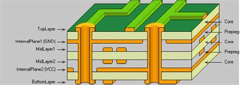
1. Define the Layer Stack-up
The layer stack-up defines the arrangement of copper and insulating layers in your PCB. Work with your manufacturer to determine the optimal stack-up for your design, considering factors such as:
- The number and thickness of copper layers
- The type and thickness of insulating material (e.g., FR-4, Rogers)
- The impedance requirements for controlled impedance traces
- The desired board thickness and aspect ratio
2. Partition the Board into Functional Blocks
Divide your circuit into functional blocks based on their purpose and requirements. For example, separate analog and digital sections, high-speed and low-speed signals, and power and ground planes. This helps minimize interference and simplifies routing.
3. Route the Signals
Use the CAD software to route the signals between components according to your design rules. Follow these guidelines:
- Keep signal traces as short and direct as possible to minimize delays and reflections.
- Maintain consistent trace widths and spacing to ensure controlled impedance.
- Avoid sharp bends and corners, which can cause signal integrity issues.
- Use vias strategically to transition between layers while minimizing stub lengths.
4. Place and Route Power and Ground
Dedicate layers to power and ground planes to provide low-impedance paths for current flow. Follow these tips:
- Use wide, uninterrupted planes to minimize impedance and voltage drops.
- Place decoupling capacitors close to power pins to suppress high-frequency noise.
- Use multiple vias to connect power and ground planes to component pins.
5. Verify the Design
Before sending your design for manufacturing, perform thorough checks to verify its integrity. Use the CAD software’s built-in tools for:
- Design rule checking (DRC) to ensure compliance with manufacturing constraints.
- Electrical rule checking (ERC) to detect potential short circuits, open circuits, and other errors.
- Signal integrity analysis to simulate and optimize high-speed signals.
- Thermal analysis to identify hot spots and ensure adequate heat dissipation.

Manufacturing Your Multilayer PCB
Once your design is complete and verified, it’s time to send it for manufacturing. Choose a reputable PCB manufacturer with experience in multilayer fabrication. Provide them with the following files:
- Gerber files: The industry-standard format for PCB designs, containing information about each layer’s copper traces, pads, and vias.
- Drill files: Specifies the locations and sizes of holes to be drilled in the board.
- Bill of Materials (BOM): A list of all the components used in the design, including their quantities and specifications.
- Assembly drawings: Visual aids that show the placement and orientation of components on the board.
The manufacturing process for multilayer PCBs typically involves the following steps:
- Inner layer fabrication: The copper layers are patterned and etched according to the Gerber files.
- Lamination: The inner layers are bonded together with insulating material under high temperature and pressure.
- Drilling: Holes are drilled through the board according to the drill files.
- Plating: The holes are plated with conductive material to create vias and connect the layers.
- Outer layer fabrication: The outer layers are patterned and etched, and any additional features (e.g., silkscreen, solder mask) are applied.
- Finishing: The board is cut to its final shape and any required surface finishes (e.g., HASL, ENIG) are applied.
- Testing: The board undergoes electrical and visual inspections to ensure it meets the required specifications.

Frequently Asked Questions (FAQ)
1. What is the difference between a multilayer PCB and a single-layer or double-layer PCB?
A single-layer PCB has only one layer of conductive material (copper) on one side of the insulating substrate. A double-layer PCB has two layers of copper, one on each side of the substrate. In contrast, a multilayer PCB has three or more layers of copper, with insulating material separating each layer. Multilayer PCBs offer increased circuit density, improved signal integrity, and better thermal management compared to single-layer or double-layer boards.
2. How do I determine the number of layers needed for my PCB?
The number of layers needed depends on several factors, including the complexity of your circuit, the number of components, the routing density, and the signal speed and integrity requirements. As a general guideline, simple designs with few components can use a 4-layer board, while more complex designs may require 6, 8, or even more layers. Consult with your PCB manufacturer and consider the trade-offs between layer count, board size, and manufacturing cost to determine the optimal number of layers for your application.
3. What are vias, and why are they important in multilayer PCBs?
Vias are small holes drilled through the PCB and plated with conductive material. They serve to interconnect the different layers of the board, allowing signals and power to pass between them. Vias are essential in multilayer PCBs because they enable the routing of signals in three dimensions, which is necessary to achieve high circuit density and signal integrity. However, vias also introduce discontinuities and stubs that can affect signal quality, so they must be used strategically and with care.
4. What is controlled impedance, and why is it important in multilayer PCBs?
Controlled impedance refers to the technique of designing PCB traces to have a specific characteristic impedance, typically 50 or 100 ohms. This is important for high-speed digital signals because it helps to minimize reflections, crosstalk, and other signal integrity issues. In multilayer PCBs, controlled impedance is achieved by carefully controlling the width and spacing of traces, as well as the thickness and dielectric constant of the insulating layers. Proper controlled impedance routing is essential for ensuring reliable high-speed performance in multilayer PCBs.
5. What are some best practices for designing multilayer PCBs?
Some best practices for designing multilayer PCBs include:
- Defining a clear layer stack-up that optimizes signal integrity and manufacturability.
- Partitioning the board into functional blocks to minimize interference and simplify routing.
- Keeping signal traces as short and direct as possible, with consistent widths and spacings.
- Dedicating layers to power and ground planes to provide low-impedance current paths.
- Using vias strategically to minimize stub lengths and maintain signal integrity.
- Performing thorough design rule checks and simulations to verify the design before manufacturing.
By following these best practices and working closely with your PCB manufacturer, you can ensure a successful and reliable multilayer PCB design.
Conclusion
Multilayer PCBs are essential for today’s complex electronic systems, offering increased circuit density, improved signal integrity, and better thermal management compared to simpler board designs. When determining your multilayer PCB requirements, consider factors such as circuit complexity, signal speed and integrity, power distribution, thermal management, manufacturing constraints, and cost. Use CAD software to design your board according to best practices for layer stack-up, signal routing, power and ground distribution, and design verification. Choose a reputable PCB manufacturer with experience in multilayer fabrication, and provide them with all the necessary files and documentation. By following these guidelines and working closely with your manufacturer, you can ensure a successful and reliable multilayer PCB for your product.


Leave a Reply