Introduction to PCB Prototypes
Printed Circuit Board (PCB) prototypes are essential in the electronics industry for testing and validating designs before mass production. PCB Prototyping allows engineers and designers to identify potential issues, optimize performance, and ensure the functionality of their circuits. In this article, we will explore the process of manufacturing and assembling PCB Prototypes, focusing on the popular 3+3 configuration.
What are PCB Prototypes?
PCB prototypes are early versions of printed circuit boards that are designed and fabricated to test and validate the functionality of an electronic circuit. These prototypes are crucial in the development process as they allow engineers to identify and fix any issues before mass production, saving time and resources in the long run.
Why are PCB Prototypes Important?
PCB prototypes serve several important purposes in the electronics industry:
- Design Validation: Prototypes allow engineers to test their designs and ensure that the circuit functions as intended.
- Functionality Testing: By assembling the prototype, engineers can verify the performance of the circuit under real-world conditions.
- Optimization: Prototypes enable engineers to identify areas for improvement and optimize the design for better performance, reliability, and cost-effectiveness.
- Error Detection: Testing prototypes helps identify any errors or issues in the design, allowing for necessary corrections before mass production.
Understanding the 3+3 PCB Prototype Configuration
The 3+3 PCB prototype configuration refers to the number of layers and the composition of the printed circuit board. In this configuration, the PCB consists of three layers of conductive material (typically copper) and three layers of insulating material (typically FR-4).
Layers in a 3+3 PCB Prototype
- Top Layer: This is the outermost layer of the PCB, where components are placed and soldered.
- Inner Layer 1: The first inner layer is used for signal routing and power distribution.
- Inner Layer 2: The second inner layer is also used for signal routing and power distribution.
- Bottom Layer: This is the opposite side of the top layer, where additional components can be placed and soldered.
The three insulating layers are placed between the conductive layers to prevent short circuits and ensure proper electrical insulation.
Advantages of the 3+3 PCB Prototype Configuration
The 3+3 PCB prototype configuration offers several advantages over other configurations:
- Increased Routing Density: With three conductive layers, the 3+3 configuration allows for higher routing density compared to two-layer PCBs.
- Improved Signal Integrity: The additional layers help reduce electromagnetic interference (EMI) and improve signal integrity.
- Enhanced Thermal Management: The inner layers can be used for power distribution, which helps dissipate heat more effectively.
- Cost-Effective: The 3+3 configuration strikes a balance between performance and cost, making it a popular choice for many applications.

Manufacturing Process of PCB Prototypes
The manufacturing process of PCB prototypes involves several steps, each of which is critical to ensuring the quality and functionality of the final product.
Step 1: Design and Layout
The first step in manufacturing a PCB prototype is to create a schematic design and layout using specialized software such as Altium Designer, Eagle, or KiCad. The schematic design represents the electrical connections between components, while the layout determines the physical placement of components and routing of traces on the PCB.
Step 2: Fabrication
Once the design and layout are finalized, the PCB prototype is fabricated using the following sub-steps:
- Printing the Circuit Pattern: The circuit pattern is printed onto a thin layer of copper foil laminated onto the insulating substrate material.
- Etching: The unwanted copper is removed using a chemical etching process, leaving only the desired circuit pattern.
- Drilling: Holes are drilled into the PCB to accommodate through-hole components and vias.
- Plating: A thin layer of copper is deposited onto the drilled holes to ensure electrical connectivity between layers.
- Solder Mask Application: A protective solder mask is applied to the PCB to prevent short circuits and improve the solderability of the pads.
- Silkscreen Printing: Text and symbols are printed onto the PCB for component identification and assembly guidance.
Step 3: Assembly
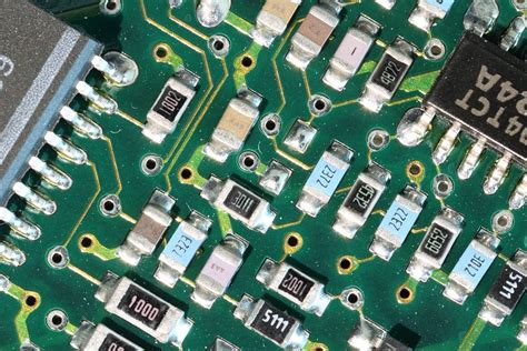
After the PCB prototype is fabricated, the components are assembled onto the board. This process can be done manually or using automated assembly machines, depending on the complexity of the design and the quantity of prototypes required.
- Solder Paste Application: A precise amount of solder paste is applied to the pads on the PCB where surface-mount components will be placed.
- Component Placement: Surface-mount components are placed onto the solder paste using pick-and-place machines or manually.
- Reflow Soldering: The PCB is heated in a reflow oven, melting the solder paste and creating a permanent electrical and mechanical connection between the components and the PCB.
- Through-Hole Component Placement: Through-hole components are inserted into the drilled holes on the PCB.
- Wave Soldering: The PCB is passed over a wave of molten solder, which fills the through-holes and creates a connection between the components and the PCB.
- Inspection and Testing: The assembled PCB prototype is inspected visually and tested electrically to ensure proper functionality and quality.

Advantages of Professional PCB Prototype Manufacturing and Assembly Services
While it is possible to manufacture and assemble PCB prototypes in-house, many companies choose to outsource these tasks to professional PCB prototype manufacturing and assembly services. Some of the advantages of using these services include:
- Expertise and Experience: Professional PCB prototype manufacturers have the expertise and experience necessary to produce high-quality prototypes consistently.
- Advanced Equipment: PCB prototype manufacturers invest in advanced equipment and technology to ensure the best possible results.
- Time and Cost Savings: Outsourcing PCB prototype manufacturing and assembly can save time and costs associated with maintaining an in-house facility.
- Scalability: Professional services can easily scale up production to meet increased demand for prototypes.
- Quality Assurance: PCB prototype manufacturers adhere to strict quality control standards to ensure the reliability and functionality of the prototypes.

Choosing the Right PCB Prototype Manufacturer
When selecting a PCB prototype manufacturer, consider the following factors to ensure the best possible results:
- Experience and Reputation: Choose a manufacturer with a proven track record of producing high-quality PCB prototypes.
- Technical Capabilities: Ensure that the manufacturer has the necessary equipment and expertise to handle your specific requirements.
- Turnaround Time: Consider the manufacturer’s turnaround time to ensure that your prototypes are delivered within your project timeline.
- Customer Support: Look for a manufacturer that offers excellent customer support and communication throughout the prototyping process.
- Pricing: Compare pricing from multiple manufacturers to ensure that you are getting a competitive rate without compromising on quality.
Common Challenges in PCB Prototype Manufacturing and Assembly
Despite the many advantages of PCB prototyping, there are some common challenges that engineers and manufacturers may face during the process:
- Design Complexity: As PCB designs become more complex, the manufacturing and assembly process becomes more challenging, requiring advanced equipment and expertise.
- Miniaturization: The trend towards miniaturization in electronics can make PCB prototyping more difficult, as smaller components and tighter tolerances are required.
- Material Selection: Choosing the right materials for the PCB prototype is crucial for ensuring performance and reliability, but can be challenging given the wide range of available options.
- Voltage and Current Requirements: Ensuring that the PCB prototype can handle the required voltage and current levels is essential for proper functionality and safety.
- Electromagnetic Compatibility (EMC): Designing and manufacturing PCB prototypes that meet EMC requirements can be challenging, particularly for high-frequency or high-power applications.
Future Trends in PCB Prototype Manufacturing and Assembly
As technology continues to advance, the PCB prototyping industry is expected to evolve to keep pace with new requirements and challenges. Some of the future trends in PCB prototype manufacturing and assembly include:
- Increased Adoption of 3D Printing: 3D printing technology is becoming increasingly popular for PCB prototyping, enabling faster turnaround times and greater design flexibility.
- Advanced Materials: New materials, such as high-frequency laminates and flexible substrates, are being developed to meet the demands of emerging applications.
- Automation and AI: Automation and artificial intelligence (AI) are expected to play a larger role in PCB prototyping, enabling faster and more efficient manufacturing and assembly processes.
- Internet of Things (IoT) Integration: As the IoT continues to grow, PCB prototypes will need to be designed and manufactured to accommodate the unique requirements of connected devices.
- Environmental Sustainability: There is a growing emphasis on environmentally sustainable practices in PCB prototyping, such as the use of lead-free materials and the adoption of green manufacturing processes.
FAQs
- What is the typical turnaround time for a 3+3 PCB prototype?
-
The turnaround time for a 3+3 PCB prototype can vary depending on the complexity of the design and the manufacturer’s workload. However, most professional PCB prototype manufacturers can deliver 3+3 prototypes within 5-10 business days.
-
How much does it cost to manufacture and assemble a 3+3 PCB prototype?
-
The cost of manufacturing and assembling a 3+3 PCB prototype depends on factors such as the size of the PCB, the number of components, and the quantity of prototypes ordered. On average, a single 3+3 PCB prototype can cost between $100 and $500, with prices decreasing for larger quantities.
-
Can I manufacture and assemble PCB prototypes in-house?
-
Yes, it is possible to manufacture and assemble PCB prototypes in-house if you have the necessary equipment, expertise, and resources. However, for most companies, outsourcing PCB prototyping to a professional manufacturer is more cost-effective and efficient.
-
What are the most common materials used for 3+3 PCB prototypes?
-
The most common materials used for 3+3 PCB prototypes are FR-4 laminate for the insulating layers and copper for the conductive layers. FR-4 is a glass-reinforced epoxy laminate that offers good mechanical and electrical properties, while copper is chosen for its excellent conductivity and solderability.
-
How do I choose the right PCB prototype manufacturer for my project?
- When choosing a PCB prototype manufacturer, consider factors such as their experience, technical capabilities, turnaround time, customer support, and pricing. It is also a good idea to read reviews and ask for recommendations from colleagues or industry professionals to ensure that you select a reputable and reliable manufacturer.
Conclusion
PCB prototyping is a critical step in the electronics design process, enabling engineers to test and validate their designs before moving to mass production. The 3+3 PCB prototype configuration offers a balance of performance and cost-effectiveness, making it a popular choice for many applications.
By understanding the manufacturing and assembly process, as well as the advantages of professional PCB prototype services, engineers can ensure that their designs are brought to life efficiently and effectively. As technology continues to evolve, staying informed about future trends and challenges in PCB prototyping will be essential for staying competitive in the electronics industry.
| Characteristic | Description |
|---|---|
| Layers | 3 conductive layers (copper) and 3 insulating layers (FR-4) |
| Routing Density | Higher compared to 2-Layer PCBs |
| Signal Integrity | Improved due to additional layers and reduced EMI |
| Thermal Management | Inner layers can be used for power distribution and heat dissipation |
| Cost | Cost-effective balance between performance and price |
| Common Applications | – Automotive electronics – Industrial control systems – Medical devices – Consumer electronics |
By leveraging the benefits of 3+3 PCB prototypes and partnering with experienced manufacturing and assembly services, engineers can bring their innovative designs to life and contribute to the ever-evolving landscape of the electronics industry.


Leave a Reply